Applications and Projects in the Field Devices and Technologies

Application areas and current projects of the business unit Devices and Technologies at Fraunhofer IMS

During the last decades the research and development activities in micro- and nanoelectronics led to a continuous reduction in structure size and therefore to an increasingly growing integration density. The goal is always to further increase the functionality on a chip or a microsystem.

Fraunhofer IMS continues this trend and develops compact and efficient micro- and nanosystems in various application areas:

Pixel detectors: Project DEPFET

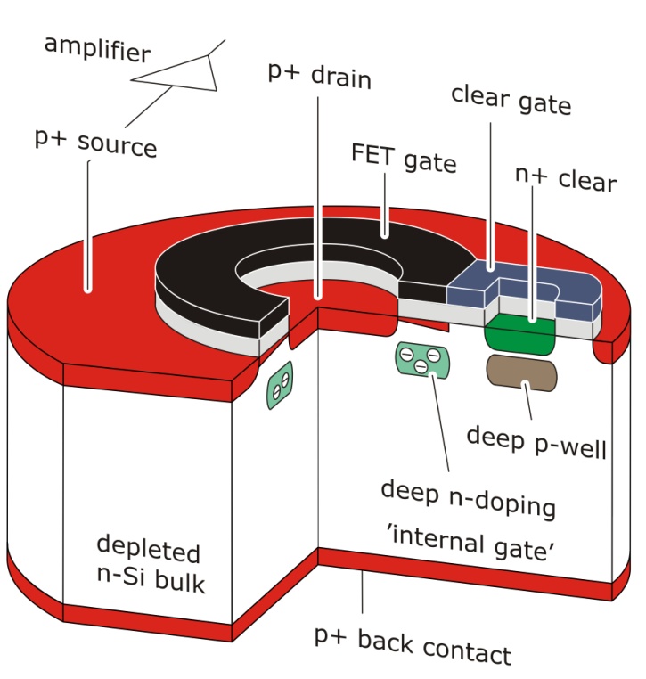
DEPFET pixel consisting of field-effect transistor with internal gate on fully-depleted silicon substrate
© Fraunhofer IMS
DEPFET pixel consisting of field-effect transistor with internal gate on fully-depleted silicon substrate

DEPFET (“depleted p-channel field-effect transistor“) detectors are extremely fast imaging pixel detectors with an excellent energy resolution, and with especially high radiation intensity. Sensors and detectors with integrated electronics for ionizing radiation find application in basic and applied research as well as in industrial analytics and quality control. A DEPFET cell consists of an operationally fully depleted silicon substrate and a field-effect transistor embedded into this same substrate.  With DEPFET detectors, the first amplification level is integrated in each pixel. This leads to a very small input capacity and therefore to a very good noise behavior of the detector. Until now, these special low-noise detectors have been only produced in the research laboratory. Together with PNSensor GmbH, Fraunhofer IMS researchers are currently developing a manufacturing process for DEPFET detectors with industrial quality standards.

To the project

High Temperatur Electronics: Project HOTMOS

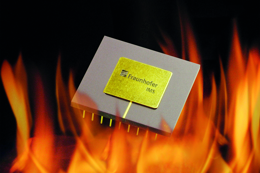
Depiction of a high-temperature integrated circuit in ceramic housing in flames
© Fraunhofer IMS
High-temperature integrated circuit in ceramic housing

In the project HOTMOS Fraunhofer IMS and Carnot CEA-LETI are working together to increase the operating range of microelectronic systems for the application in harsh environments. In this project a SOI CMOS technology platform has been developed for the application of microelectronic circuits for temperature ranges of more than 250 °C.

The high integration density of the 0.35 μm SOI CMOS enables the intelligent and compact drivers that contain on-chip controls, fault management and energy management.

To the project

Gas sensor: Project FunALD

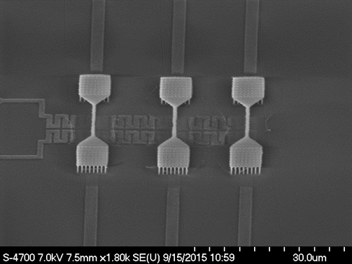
Freestanding nanowire over heizermeander structures, for examples for gas detection through resistance change
© Fraunhofer IMS
Freestanding nanowire over heater structures, for examples for gas detection through resistance change

Within the framework of the project „Functional ultrathin materials trough atomic layer deposition for the next generation of nanosystems technology” (short: FunALD) a new kind of material production, especially for sensor technology, is being researched, the “Atomic Layer Deposition” (short:ALD). New organometallic raw materials (“precursors”) for the ALD process are being developed, test structures on the basis of layers and layer sequences are being designed and manufactured, and measurement processes are being developed to characterize layers and layer sequences systematically.

The goal of this three-year project is to develop ultrathin, functional materials on the basis of ALD technology for applications in the area of mechanical sensors and gas sensor systems.

To the project

HF-Transponder: Project MARIE

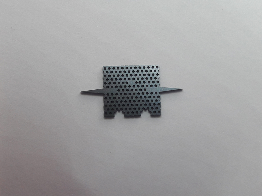
Resonator from high resistance silicon manufactured in the MST Lab&Fab
© Fraunhofer IMS
Resonator from high resistance silicon manufactured in the MST Lab&Fab

Fraunhofer IMS is participating within the EU research project „MARIE“(MAteRIal TranscEiver) with the production of dielectrical resonators (RFID tags) for sub-millimeter localization. Fraunhofer IMS is manufacturing the high-frequency resonators in the microsystem technology Lab&Fab. Objects with these “tags” can be localized in a field of high-frequency. The goal is to achieve a better location accuracy of less than a millimeter.

To the project

Nanoelektrode array: Project ZellMOS

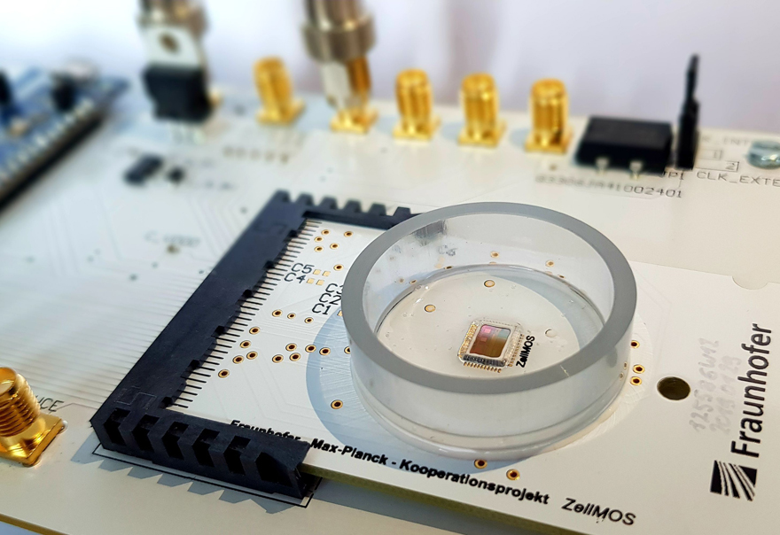
For the measurement of biological celld the CMOS nanoelectrode array is electrically connected and immersed into a sealed fluid reservoir.
© Fraunhofer IMS
For the measurement of biological cells the CMOS nanoelectrode array is electrically connected and immersed into a sealed fluid reservoir.

In the Fraunhofer and Max-Planck cooperation project ZellMOS researchers from Fraunhofer IMS, the Max-Planck Institute for Medical Research and the University Clinic Heidelberg are working on electrical contact of living cells via semiconductor circuits. For this purpose, CMOS nanoelectrode arrays are  produced using metal oxide semiconductors. In a joint effort the researchers of both research organizations want to demonstrate a direct, efficient, bidirectional and long-term stable electronic coupling between living cells and CMOS-integrated 3D electrodes.

To the project

Point-of-Care-Diagnostics: Project PoC-ID

Membrane structure of the manufactured bio MEMS
© Fraunhofer IMS
Microscopic image of the manufactured bio MEMS

In the project PoC-ID a compact measurement device on the basis of a BioMEMS sensor is being developed for the diagnosis of infections with the respiratory syncytial virus (RSV) in newborns. For this purpose Fraunhofer IMS is working together with its project partners on a sensor that detects the existence of the virus and the concentration of several infection parameters in one sample. The process development and the production of the MEMS sensor is carried out in the in-house microsystems technology Lab&Fab. The functional structure of the MEMS sensor consists of a few micrometers thin membrane which is cause to vibrate via piezoelectric effects. This membrane is additionally coated with capture molecules that selectively bind infection parameters or virus samples. Through the binding of the molecules the mass of the membrane is increasing and results in a reduction of the vibration frequency. This vibration frequency change is detected by an in-house developed electronic evaluation units and provides conclusions on the existence and the concentration of the sample parameters.

To the project

This might interest you

ZellMOS

In the interdisciplinary Fraunhofer Max Planck cooperation project ZellMOS, chip designers, process engineers and biophysicists are developing a CMOS nanoelectrode array.

FunALD

Fraunhofer IMS offers a large selection of modern ALD processes for innovative sensor technology.


Large-area DEPFET-detectors

Fraunhofer IMS is developing a customer-specific CMOS process for the production of large-area X-ray sensors.

Overview Pages

Devices and Technologies (Home)

Fraunhofer IMS offers the optimal conditions for the development of innovative microelectronic and micromechanic devices and systems.

Technologies

Customer-specific CMOS process, high-temperature ICs, MEMS and post-CMOS processing, atomic layer deposition (ALD), 3D-Integration

Customer Benefits

Our offers for customer-oriented solutions – from the process development up series production

Download