 Fraunhofer Institute for Microelectronic Circuits and Systems
Vision 12 µm: The new, extremely small microbolometers of Fraunhofer IMS
Uncooled infrared-detectors measure the thermal radiation of their environment and depicture the temperature distribution of a scene. Core of these detectors is a thermal sensor element, the microbolometer. Now the Fraunhofer Institute for Microelectronic Circuits and Systems IMS has developed a new generation of microbolometers: extra small and therefore especially affordable. The small size is a large advantage for mobile applications. These tiny sensors can be applied in, for example, helmet cameras of firefighters. The possibility to produce them cost-effective, makes them especially interesting for the mass market. Thanks to an innovative structure the new microbolometers are despite of their small size extremely efficient.
The new development is constructed like this: As intelligent substrate serve 200 mm wafer, made of silicon and with integrated readout circuit. The microbolometers are located on this and measure the infrared-radiation by absorbing them over their surface. They are embedded in a vacuum case which ensures that heating can result.
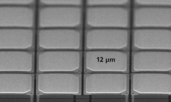
The latest state of technology is so far a microbolometer with a pixel pitch of 17 µm. At Fraunhofer Institute a reduction to pixel pitch 12 µm succeeded. “Thereby we achieved a halving of the surface” says Dr. Dirk Weiler, leader of the business unit “IR Imagers” at Fraunhofer IMS. “The challenge was to maintain the temperature sensitivity even though the surface was halved.” This became possible due to an innovative, registered for patent microbolmeter structure with a maximum absorbing-membrane in the middle and without additional webs for thermal insulation in the edge region. The conventional 17 µm microbolometers have a filling factor of 70 percent. “We have the possibility to bring the filling factor up to nearly 100 percent, due to the innovative structure of our microbolmeters”, explains Dr. Weiler. That way the efficiency of the absorption rises.
The reduction provides obvious advantages: The production costs decrease because almost twice as much chips fit on a wafer. Even the camera lens becomes more cost-efficient because the image area is smaller. Because of this higher resolving Imager are possible in the first place. The new structure even allows subsequent generations to produce even smaller microbolometers in the future.
A firefighter is for example able to search for glow nests with a smaller, handier camera – or even a helmet camera. So that the hands could be free for the rescue operation.
Drivers or the electronics of autonomous vehicles could recognize pedestrians in the night without turning on high beam. The affordable technology would not only be reserved for cars from the premium segment. Also, craftsmen could control for example an underfloor heating with the mini sensor, without opening the whole floor screed, or check the building insulation. Because many technical devices get warm, right before they break, the new micobolometers are also suitable for preventive maintenance. Medical applications are conceivable as well: the wide-ranging infrared-detector can determine circulatory disturbances at cold parts of the body and make inflammations visible at warm parts of the body.
“Fraunhofer IMS in Duisburg is the only Institute in Germany that manufactures microbolometers”, says Dr. Weiler. “We are looking forward to industry partners for the further development and application of our new version 12 µm.”
Fraunhofer Institute of Microelectronic Circuits and Systems IMS
Since 30 years, scientists at Fraunhofer IMS in Duisburg deal with the development of microelectronic circuits, electronic systems, microsystems and sensors. Because of its comprehensive know-how, the access to technology and the high-quality development work the Institute is a worldwide recognized partner for the industry. In eight business units Fraunhofer IMS is dedicated to applied research, advance development for products and their applications. Stable, efficient and marketable technologies and procedures that are used in extremely many branches take center stage in contract work.