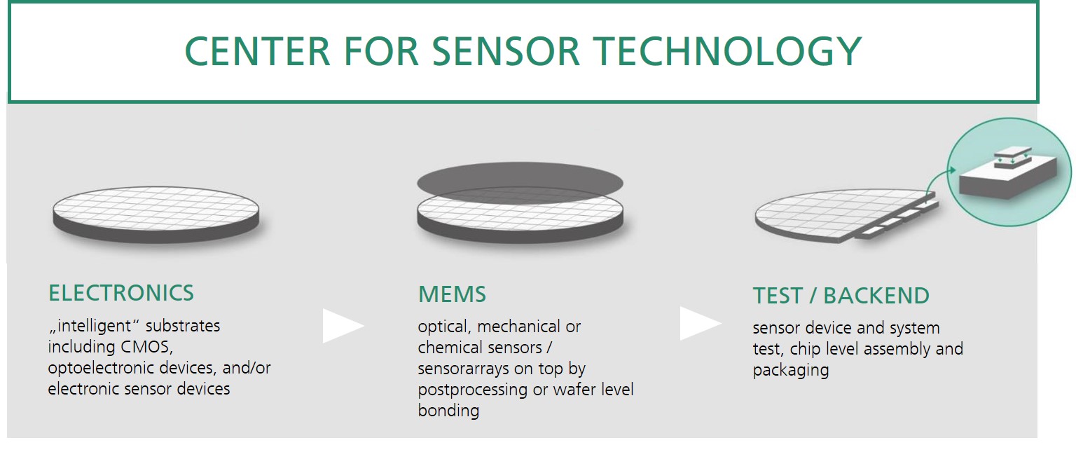
In a clean room area of 2000 m² - the Center of Sensor Technology - we fabricate novel innovative sensors with ultra-modern equipment and technologies. Our clean room offers a wide range of technologies:
Center for Sensor Technology

- Electronics for ultra-clean CMOS-compatible processes, CMOS-integration (also from external foundries) and the integration of electro-optical sensors
- MEMS for the integration of MEMS processes and the flexibility to integrate a wide range of different functional materials
- BackEnd for wafer and device testing and assembly / packaging of chips into package or directly on PCB.
All clean room areas of the Center for Sensor Technology are compatible with each other thanks to the uniform 200 mm silicon cassette handling. This enables us to implement the complete process chain from the bare silicon wafer to the complete sensor system.
We operate our clean rooms in two shifts, 7 days a week. Our team of experienced scientists, developers, design experts and technologists work hand in hand with you – starting with the fabrication of demonstrators and prototypes up to pre-production and pilot production.
The integration of wafers from external foundries into our process flow is our daily business. This enables us to offer optimal technological combinations and cost-effective solutions to our customers. We closely work together with various foundries.
Our clean rooms in the Center for Sensor Technology are part of the Research Fab Microelectronics Germany - Forschungsfabrik Mikroelektronik Deutschland (FMD) - a global innovation driver, consisting of eleven Fraunhofer Institutes and two Leibniz Institutes. The largest cross-location R&D association for microelectronics in Europe offers a unique competence and infrastructure diversity. The FMD bridges the gap from basic research to customer-specific product development. The FMD is supported by the Federal Ministry of Education and Research (BMBF). Forschungsfabrik Mikroelektronik Deutschland (FMD) (fraunhofer.de)
We meet the high-quality requirements of our customers by using a combination of systems, structures and the extensive know-how of our employees. To take just two examples: We have been certified according to DIN / ISO 9001 since 1995 and have already been able to demonstrate implementation and use in daily operations in various customer audits to the complete satisfaction of our customers. The MES system, which has been widely used by FMD, optimally maps the individual process steps, so that the complete production of the wafers is documented in the most precise manner and can be traced in every respect.
- ISO 9000 certified management system
- Digital production with the help of our modern MES
- Comprehensive system for process monitoring
- Experienced operators, technicians and engineers
Extract from our technology portfolio
The process modules can be combined with one another:
Elektronik
- Local 0.35µm-line for electronic semiconductor devices on bulk-silicon and SOI
- Low-noise optical sensors and sensor arrays with ultra-low dark count rate
- various ALD-, CVD- und PVD-processes and spin-coating for the integration of different functional materials
- Sacrificial layer and deep etching technologies for 3D structures
- Electroplating for functional metal structures
- Active and passive structures for infrared sensors (bolometer), pressure sensors, gas sensors, biosensors and other customer specific sensors
- wafer-wafer- and chip-wafer-bonding for heterogenious integration different devices and wafers to a single sensor system.
- Wafer test
- Device test / sensor test
- Dicing / thinning / polishing
- Assembly and packaging
