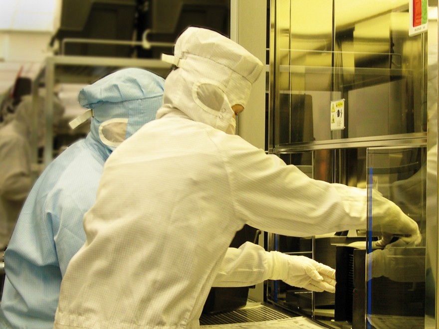
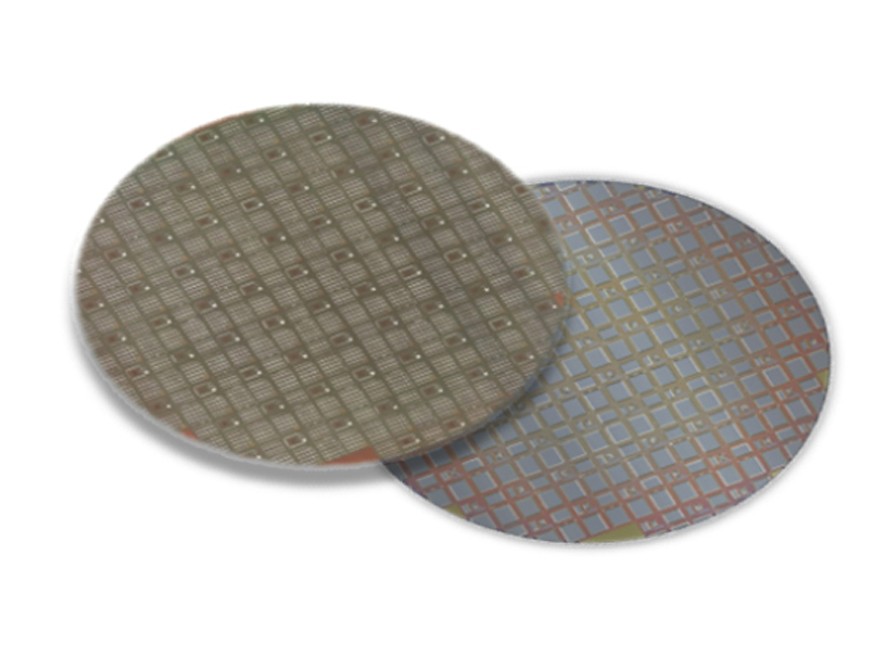
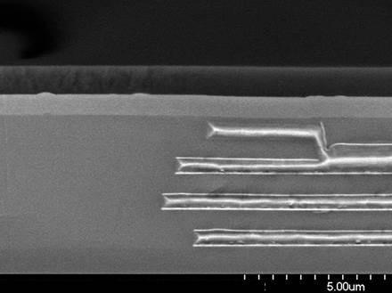
Fraunhofer IMS has more than 30 years of experience in the development of image sensors and operates a 200 mm CMOS production line for technologies down to a minimum structure size of 0.35 µm. Fraunhofer IMS develops semiconductor devices and processes from individual sub-steps to complete customer-specific image sensors. Due to the special combination of an in-house CMOS clean room and a microsystems technology Lab&Fab, the Fraunhofer IMS offers a wide variety of manufacturing processes for the realization of new technologies. Our extensive microelectronic expertise in semiconductors, image sensors and MEMS enables us to take innovative and compact microsystems through to pilot series production on request.
Image Sensors
Fraunhofer IMS optimizes image sensors in the sense of the "More-than-Moore" principle by implementing further functions, such as voltage-resistant components for the operation of integrated single photon avalanche diodes (SPAD) or develops technologies that enable the use of the circuit under harsh conditions. The production in the Fraunhofer IMS own clean room enables the optoelectronic components used in the image sensors to be adapted to the customer's requirements in close coordination with the chip designers in order to realize the best possible result for them.
Furthermore, Fraunhofer IMS develops and manufactures both analog and digital silicon photomultipliers (SiPM) as CMOS image sensors for the detection of single or few photons in various applications, e.g. the nuclear medicine procedure of positron emission tomography (PET). SiPM are based on SPAD technology and exploit the extreme sensitivity and speed of the diodes.
Another example of customized image sensors are backside illumination sensors (BSI sensors) with the latest bonding technology for highly sensitive photodetectors. BSI sensors are characterized above all by their enhanced image quality and are therefore indispensable in consumer electronics and smartphones. BSI technology can be used to generate large 2D SPAD matrices, which have enormous advantages when the detectors are used as LiDAR sensors in road traffic. In addition, Fraunhofer IMS offers CMOS-CCD structures and sensors with extremely high dynamic range by integrating CCDs into the CMOS process and performing all signal processing and sensor control internally.
The integration of the CCD into the CMOS process allows direct parallel signal processing and A/D conversion on the chip, thus minimizing parasitic interference effects. The main application area for the CMOS CCDs is in the field of time-delay integration (TDI) in space detectors.
In the area of other photodetectors, special photosensitive devices such as pinned photodiode (PPD) and other developed custom CMOS image sensors will be presented. These include high-resolution sensors for indirect time-of-flight applications and line sensors with high sensitivity and gating or short-pulse capability for spectroscopy applications.
Details about image sensors at Fraunhofer IMS can be found in the links below.


