

Gas sensors have become indispensable in many areas of the economy and everyday life. They detect diesel and gas exhaust within the outside air and prevent pollutants from coming into the car interior through the automatic control of the ventilation system. In food production, they monitor the ammonia concentration in cooling systems and in factory halls they monitor the emission of methane from the pipeline network. Air quality sensors and sensors in measurement systems detect toxic and explosive gas and against leakage of dangerous pollutants.
Currently commercially available sensors are not sensitive enough for many applications and have a high cross-sensitivity, which means that they also respond to other, not desired, substances. The key to more sensitive, specific and cost-efficient sensors can be new, ultrathin materials structured within nanometer range.
About FunALD
Within the project FunALD a new kind of material production, especially for sensor technology, is being researched – the atomic layer deposition (short: ALD). With the ALD process the material layers can be deposited and structured ultrathin – atomic layer for atomic layer. New organometallic raw materials (“precursors”) are developed for the ALD process, test structures based on layers and layering sequences are designed and manufactured and measurement processes are developed to specifically characterize the layers and layering sequences. The measurement processes are designed to enable the suitability of the ALD layers for the validation later application in sensor systems (especially for gases) and therefore also enabling a targeted optimization.
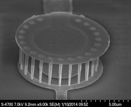
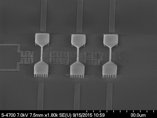
Moreover, its is possible to build freestanding three-dimensional devices using the ALD technology. These self-supporting nanowires are perfectly suited for ultrasensitive gas- or biosensors.
The findings of the project are exploited by the fact that optimized layer sequences are installed at the Fraunhofer IMS as processes that are available to the sensor development industry. Processes for precursors, layer sequences or measuring methods are available directly for transfer to the user industry.

