
The Fraunhofer IMS can rely on 30 years of experience in the field of microelectronic technology development and offers optimal conditions for the development of innovative microelectronic and micromechanical devices and systems through its technologies, infrastructure and cooperation models.
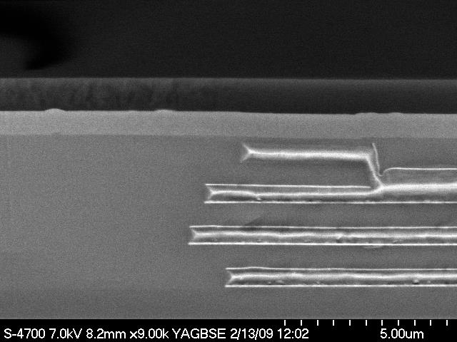
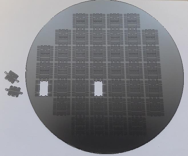
One feature of Fraunhofer IMS is the special infrastructure consisting of a 0.35 µm CMOS line and a microsystems technology Lab&Fab. This infrastructure enables development of new technology areas through the combination of CMOS and MEMS (or NEMS) up to pilot series production. This way, innovative and compact microsystems can be produced through post-CMOS processes and find application fields in the areas of medicine, industry, automotive, aerospace and in consumer electronics. One example is the post-CMOS processing for the connection of highly sensitive optical elements with asuitable readout circuit.
Our customer benefits include every topic area in the field of CMOS and MST technology from the concept and component development over the development of individual process steps up to the complete customer-specific process. Individual process steps in the microsystems technology Lab&Fab range from the deposition and structuring of layers over lithography and etching processes to electroplating and 3D-Integration.
For the electric characterization of CMOS and MEMS devices the field Devices and Technologies has suitable test and measuring stations available. Apart from the CMOS and MST clean rooms Fraunhofer IMS also offers diverse customer benefits in the area of back-end processing of microelectronic devices and systems. Our services & know-how includes the entirety of steps for assembly and packaging of microelectronic devices.
