

Intercellular communication processes in healthy organisms as well as in tumor tissue have been investigated for decades but are still not understood in detail. In order to gain new insights into the electrical signal processing of individual cells and cell networks, a microchip is developed that can process biological signals with a high signal to noise ratio.
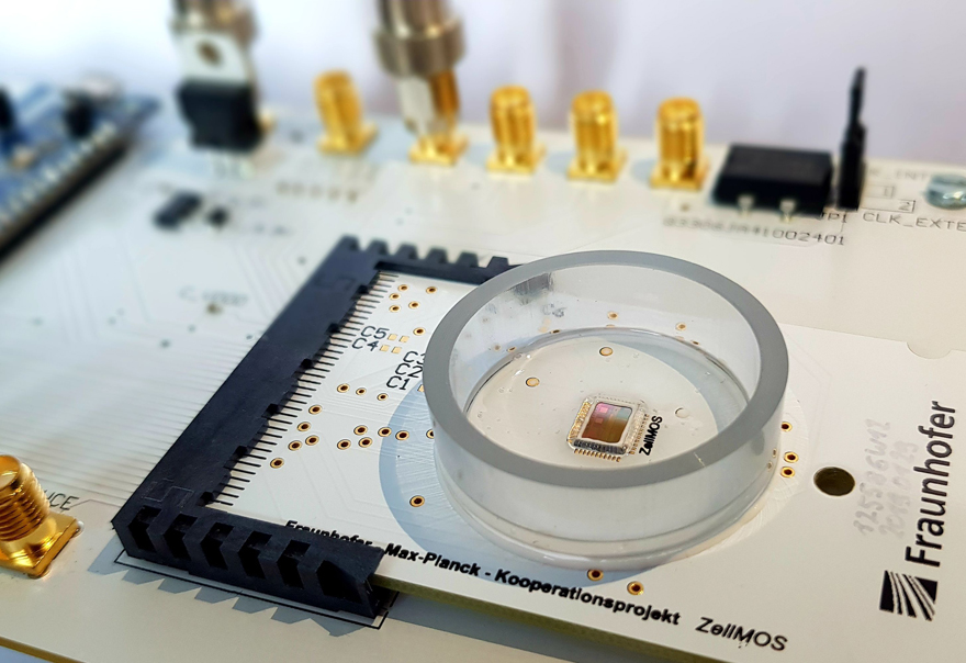
In the Fraunhofer Max Planck cooperation project ZELLMOS, scientists from the Fraunhofer IMS, the Max Planck Institute for Medical Research and the University Hospital Heidelberg are working together on the development and evaluation of a component for bidirectional electrical cell contact. A CMOS nanoelectrode array – a combination of an integrated CMOS circuit and three-dimensional nanostructures- enables highly sensitive signal acquisition of electrical bio-signals.
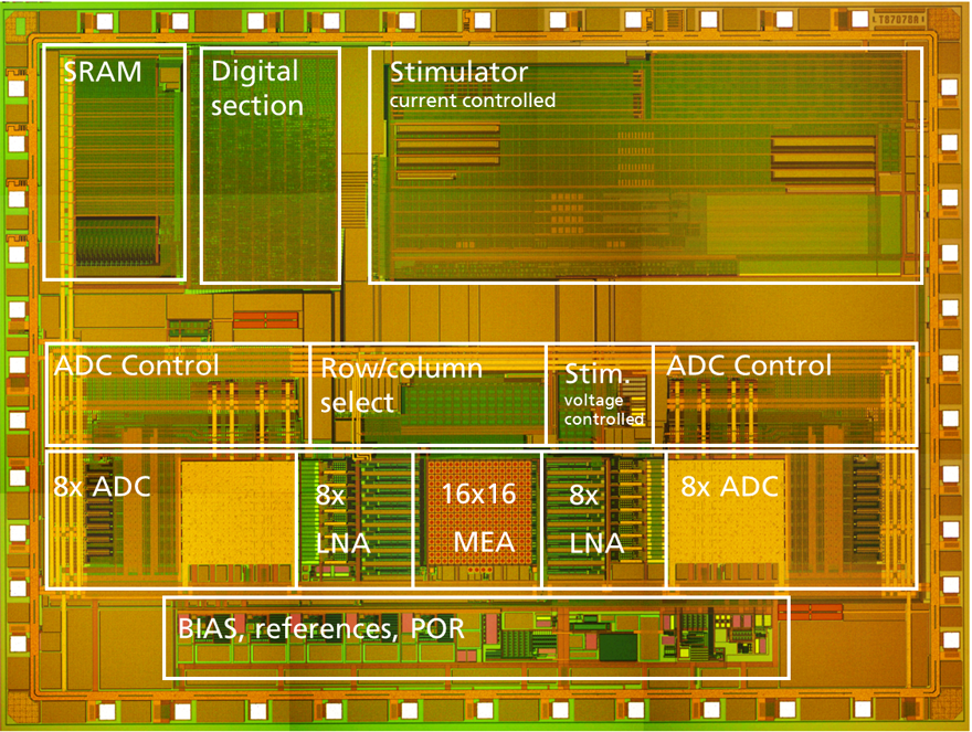
For the evaluation of cell signals, a CMOS chip was designed which drives an array of 16 x 16 electrodes. Circuits for stimulation and recording of electrical signals, a digital part and a memory unit are integrated in the chip. The amplification and digitization of the signals take place in the immediate vicinity of the signal generation, so that even the smallest signals can be processed.
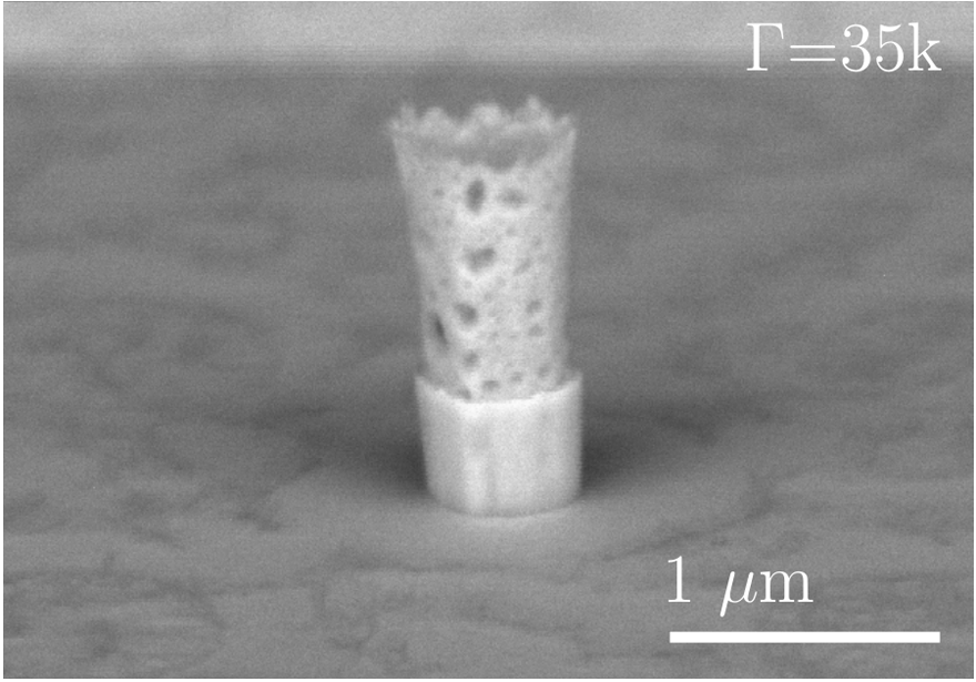
Nanoelectrodes are specifically applied to each electrode of the chip in a post-CMOS process. Vertical nano-needles penetrate the cell membrane. Thus, even the smallest signals inside the cell can be picked up by the CMOS nanoelectrode array. The shape and size of the nanoelectrodes can be adjusted to optimize cell contact.
The CMOS nanoelectrode array is used to investigate the mechanical and electrical contact of different electrogenic cells. The surface of the entire system is biofunctionalized and cell cultures are applied to it. The communication processes of the cells are analyzed in detail. This includes, for example, the investigation of newly discovered intercellular communication pathways, the so-called tunneling nanotubes (TNT).
Furthermore, innovative sensors and implants based on CMOS nanoelectrode arrays could be developed in the future.
Promotion
Funded within the Fraunhofer Max Planck Cooperation Program
