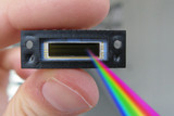
UV-transparent coating for image sensors
Image sensors as used in cell phones are partially color-blind. This is because of their coating, which prevents UV light from passing through. CMOS chips have as a result not been suitable for spectroscopy up to now. A new production process makes the coating transparent – and the sensors suitable for special applications.
They have been used as standard in multimedia electronics for a long time, and now they are making rapid inroads in high performance applications: CMOS image sensors are no longer only used in cell phones and digital cameras. The automotive industry, for instance, has discovered the potential of optical semiconductor chips and is increasingly using them in driver assistance systems – from parking aids and road lane detection to blind-spot warning devices. In special applications, however, the sensors that convert light into electrical signals have to cope with diffi cult operating conditions, for example high temperatures and moisture.
For this reason, CMOS devices are covered with a silicon nitride coating. This chemical compound forms hard layers which protect the sensor from mechanical influences and the penetration of moisture and other impurities. The protective coating is applied to the sensor in the final stage of CMOS semiconductor production. The process is called passivation, and is an industry requirement. Unfortunately, up to now this passivation has entailed a problem: the silicon nitride coating limits the range of optical applications because it is impermeable to light in the UV and blue spectral range. CMOS sensors for high-performance applications, used in special cameras are therefore partially color-blind.
Scientists at the Fraunhofer Institute for Microelectronic Circuits and Systems IMS in Duisburg have found a solution to this problem: “We’ve developed a new process step,” says Werner Brockherde, head of department at Fraunhofer IMS, “that allows us to produce a protective coating with the same properties but which is permeable to blue and UV light.” The trick is to increase the proportion of nitrogen in the coating. “This reduces the absorption of shortwave light,” explains Brockherde.
In simplified terms, the new coating material will absorbless light of an energy higher than blue light, which means the sensor becomes more sensitive at the blue and UV range. “This makes CMOS image sensors suitable for use in wavelength ranges down to 200 nanometers,” states Brockherde. “With standard passivation the limit was about 450 nanometers.” To change the structure of the silicon nitride for the coating, the Fraunhofer research scientists had to fine-tune the deposition parameters such as pressure and temperature.
With this process development the experts have expanded the range of applications for CMOS image technology. This could revolutionize UV spectroscopic methods, which are used in laboratories around the world, significantly improving their accuracy. Likewise, CMOS image sensors stand to take up a new role in professional microscopy, e.g. in fluorescence microscopes, providing scientists with images of even greater detail.
Download:
