Large-area DEPFET-pixel detectors

Custom CMOS process for realizing backlit DEPFET-detectors with up to 18 cm² active area.

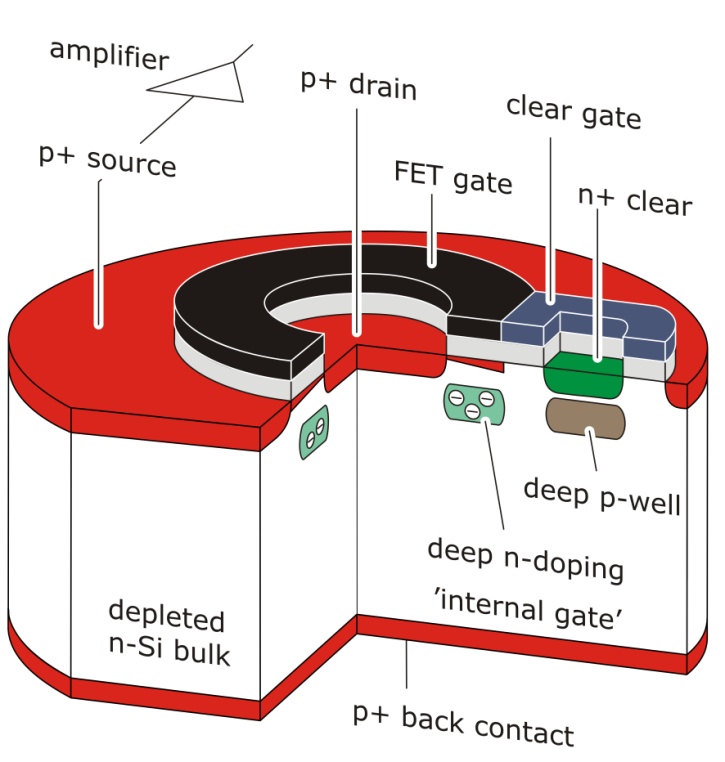
DEPFET pixel consisting of field-effect transistor with internal gate on fully-depleted silicon substrate
© Fraunhofer IMS
DEPFET pixel consisting of field-effect transistor with internal gate on fully-depleted silicon substrate
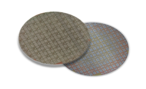
Wafer front and backside with double-sided wafer processing
© Fraunhofer IMS
Wafer front and backside with double-sided wafer processing
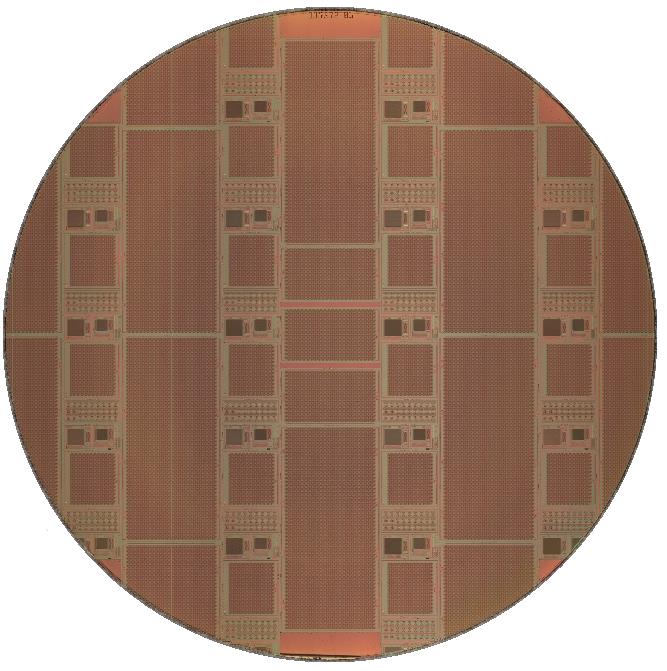
On a 8‘‘ wafer 6 large-area DEPFET detectors with 18 cm² active areas are realized by stitching.
© Fraunhofer IMS
On a 8‘‘ wafer 6 large-area DEPFET detectors with 18 cm² active areas are realized by stitching.

DEPFET detectors (“depleted p-channel field-effect transistor”) are ultra-fast pixel detectors with excellent energy resolution and high radiation hardness. Applications of X-ray sensors and detectors with integrated electronics range from fundamental and applied research to industrial analytics and quality inspection.

A DEPFET pixel consists of a field-effect transistor on a fully depleted substrate. With the first stage of signal amplification integrated in each pixel, DEPFET detectors provide low input capacitance and excellent signal-to-noise ratio. In the past these special sensors have been fabricated only in research labs. Together with PNSensor, Fraunhofer IMS is developing a fabrication process with industry quality standards.

For the application as detectors at a free-electron laser, large-area detectors with an active area of 18 cm² are currently being developed. In contrast to other BSI sensors, backside illumination of the DEPFET detectors is realized by double-sided wafer processing. Due to the large chip area of the detectors, a so-called stitching process is used where multiple layout pieces are seamlessly pieced together to one single detector chip.

The fabrication of DEPFET detectors within a CMOS line offers high process stability at short turn-around times and reduced cost. Furthermore CMOS processing offers new design options to detector developers. This enables improved detection and amplification characteristics and opens new applications in fundamental and applied research.

This might interest you

ZellMOS

In the interdisciplinary Fraunhofer Max Planck cooperation project ZellMOS, chip designers, process engineers and biophysicists are developing a CMOS nanoelectrode array.

FunALD

Fraunhofer IMS offers a large selection of modern ALD processes for innovative sensor technology.


Overview Pages

Devices and Technologies (Home)

Fraunhofer IMS offers the optimal conditions for the development of innovative microelectronic and micromechanic devices and systems.

Applications

Overview of typical development projects in the field of Devices and Technologies

Technologies

Customer-specific CMOS process, high-temperature ICs, MEMS and post-CMOS processing, atomic layer deposition (ALD), 3D-Integration

Customer Benefits

Our offers for customer-oriented solutions – from the process development up series production

Download