During development, numerous investigations are required to characterize sensors, circuits and systems. Similarly, all sensor systems developed at Fraunhofer IMS are subjected to extensive testing. Due to the variety of applications we cover, from complex integrated circuits, transponder applications, pressure, bio and other sensors to optical systems, an extensive measurement and test equipment is required to verify the development results. Fraunhofer IMS therefore has a number of specialized laboratories available for this purpose, which work with special equipment according to industrial standards and can cover all of the institute's fields of applications.
Labs and measurement equipment
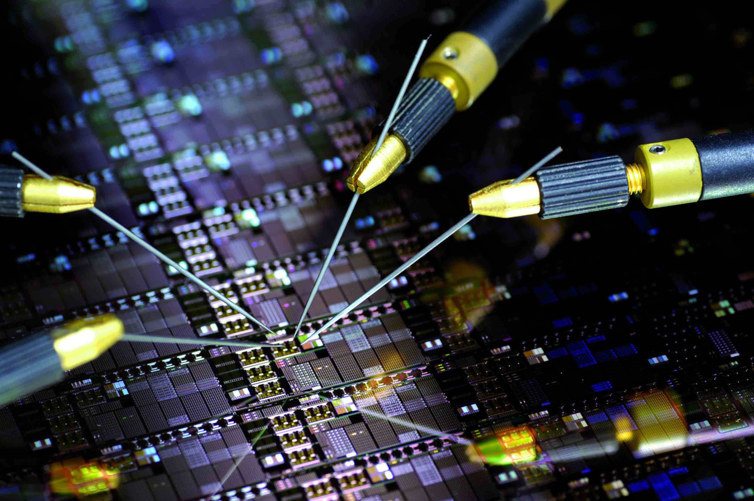
Test lab for Application Specific Integrated Circuits (ASICs)
The ASICs developed at Fraunhofer IMS can be tested automatically on wafer level with dedicated test equipment. Mixed-signal testers are available for this purpose, which use chip-specific test programs to check all specified parameters of an integrated circuit. Wafer testing is possible at temperatures from -40 °C up to 120 °C; an extension up to 300 °C is currently being prepared. In automated testing, test capacity ranges from several hundred to several million ICs per year depending on test complexity. With the appropriate handlers, packaged components can also be tested automatically.

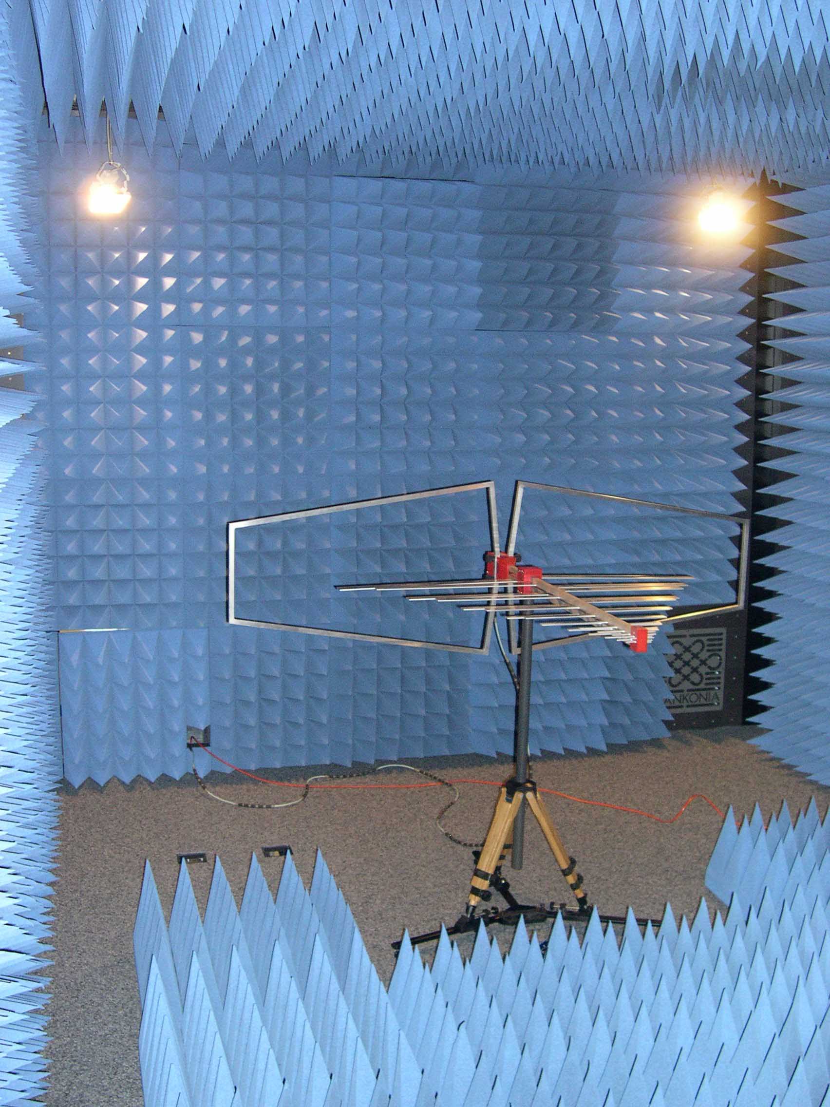
High Frequency Lab
With the transponder systems developed at the Fraunhofer IMS, the institute is pushing the limits of what is feasible in terms of the longest possible range, smallest size and the lowest possible energy consumption. The measurement equipment for systems is correspondingly demanding. To eliminate interference as far as possible, an RF measurement chamber is available which is shielded against the interference of electromagnetic fields and in which experiments on the functionality of transponders, but also on questions of electromagnetic compatibility can be investigated.
Pressure Sensor Lab
The test of pressure sensors and pressure sensor systems takes place in a special laboratory with dedicated equipment. Both pressure and temperature loads can be applied to the sensors here. Automated measurement series and long-term tests can also be carried out using appropriate software


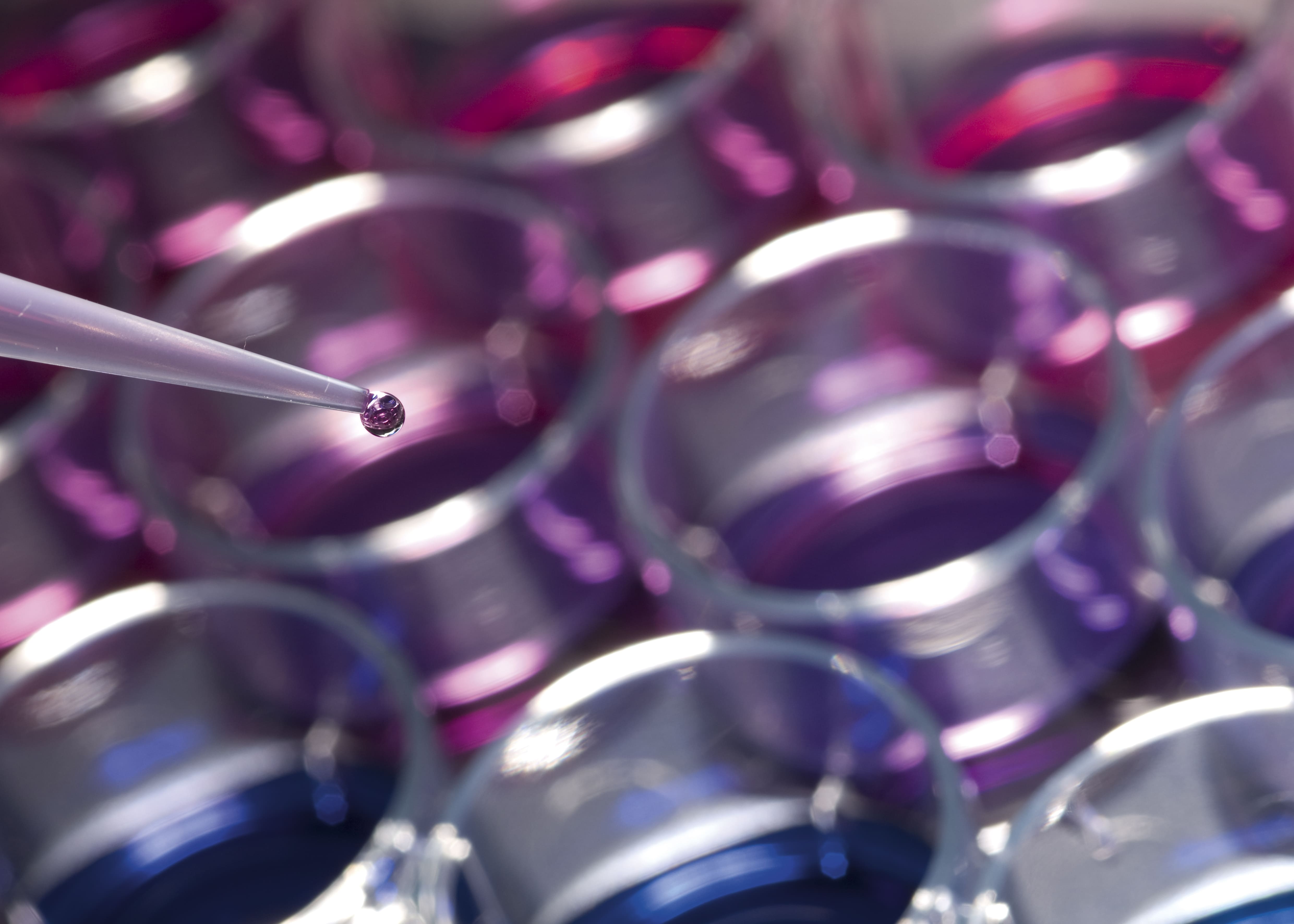
Biosensor Lab
In the field of biosensor technology, a wide range of different analytical instruments is available for the characterization of the developed biosensors. These include molecular diagnostic analyzers for performing biochemical assays, e.g. the enzyme-linked immunosorbent assay (ELISA). Furthermore, the surface of functionalized biosensors can be characterized by Raman spectroscopy, fluorescence microscopy, atomic force microscopy (AFM) and surface plasmon resonance spectroscopy (SPR-spectroscopy). Thus, the biosensors can be evaluated with standardized analytical methods established in industrial research.
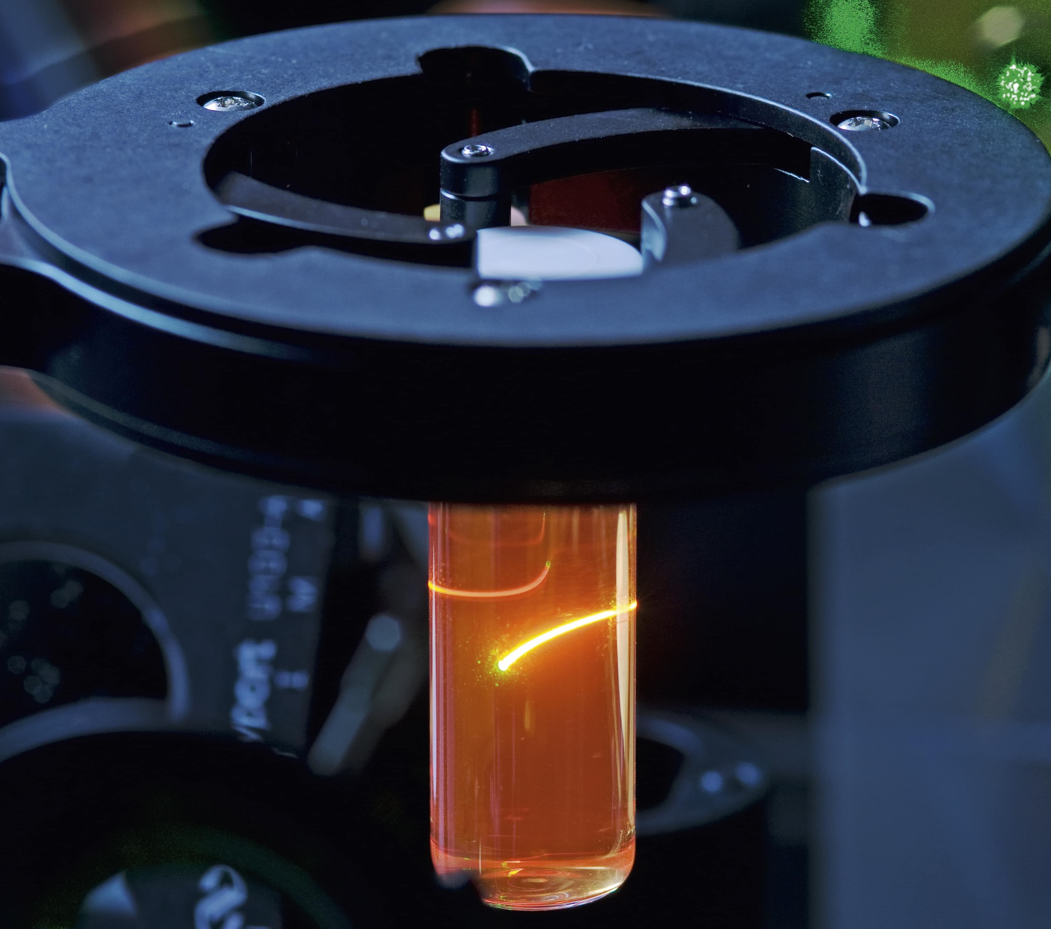
CMOS Image Sensor Lab
Fraunhofer IMS offers a comprehensive service in all areas of the development of innovative optical sensors and image sensors. For the electro-optical characterization of the sensors and the acquisition of vital parameters such as capacitance, dark current, spectral sensitivity and others according to EMVA 1288 standard, an extensive equipment is available.
