Highly sensitive image sensors with adapted microlens arrays


An important parameter of image sensors with a decisive influence on sensitivity is the fill factor. This describes the proportion of the light-sensitive area in the total area and thus the proportion of the incident photons that can be detected. SPAD (Single-Photon Avalanche Diode) -based sensors in particular usually contain very complex electronic circuits within the pixels that limit the light-sensitive area and thus the fill factor. By vertically arranging active sensor elements and the circuitry (3D integration), an improvement can already be achieved, but the pixel size is still determined by the size of the readout circuit.
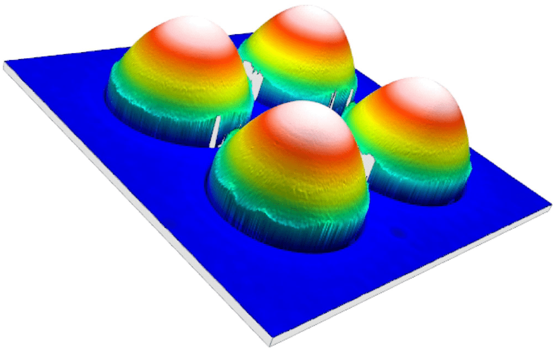
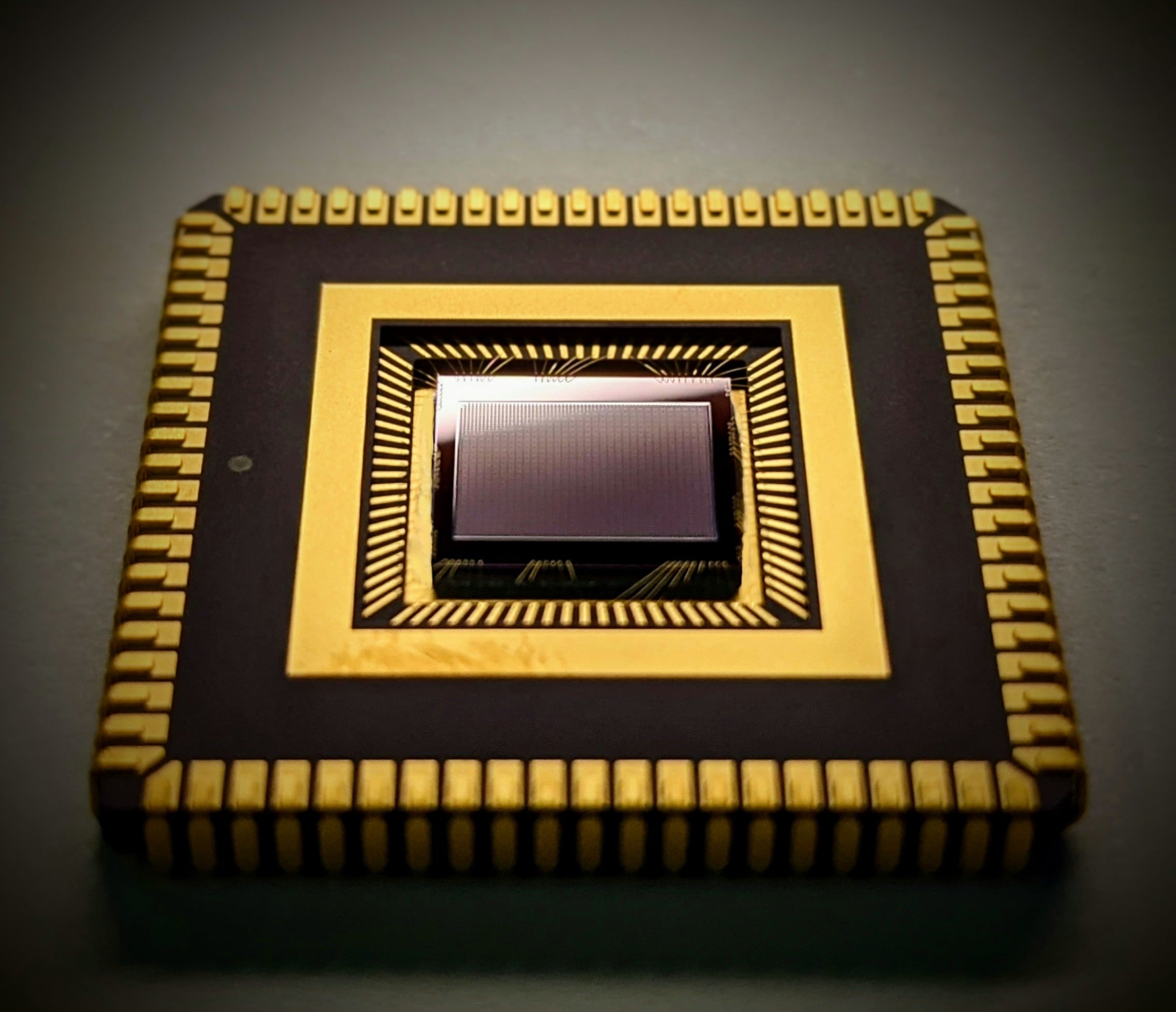
Microlenses that focus photons onto the light-sensitive surfaces of the sensor can overcome this limitation and thus bring about a decisive increase in performance. As part of the Fraunhofer-internal project "SPAD in focus", adapted microlens arrays were developed in cooperation with the Fraunhofer Institute for Applied Optics and Precision Engineering (IOF), which were directly applied to the 64 x 48 pixel CSPAD αlpha sensor and significantly increase the effective fill factor. Based on the sensor architecture, an optimized lens design was designed and simulated for this purpose. Using photolithography and reflow of photoresist, the microlens arrays adapted to the CSPAD αlpha wafer layout were mastered at wafer scale and then transferred to a replication tool. In the molding process, liquid polymer is applied to the sensor wafer and formed into the desired shape using the replication tool. Selective curing with UV light allows the areas outside the active sensor area to be kept free of polymer.
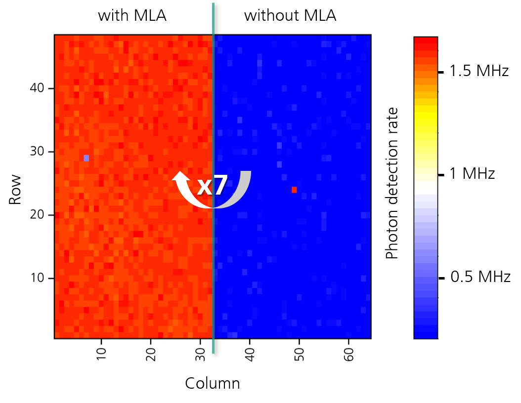
The sensors can then be separated, mounted in a housing and operated as standard. The electro-optical characterization by homogeneous defined irradiation shows an increase of the photon detection efficiency by a factor of 7. Accordingly, the lenses capture a 7-fold higher number of photons without negative influence on the sensor and focus them on the light-sensitive areas of the SPADs. Due to the possibility of replication on wafer level, high numbers of sensors can be equipped with microlens arrays and significantly improved by this method at low cost. The combination of the highly sensitive SPAD sensor device and the increased sensitivity provided by matched microlens arrays enables high-performance single-photon detection for imaging applications such as LiDAR and quantum imaging.
The Fraunhofer IMS is continuously working on the development and optimization of SPAD-based sensors and is looking for partners for applications of this technology. Please feel free to contact us!
Contact
Fraunhofer Institute for Microelectronic Circuits and Systems IMS
Michael Bollerott
Telefon: +49 203 3783-227
Michael.Bollerott@ims.fraunhofer.de
Presse
About Fraunhofer IMS
The Fraunhofer Institute for Microelectronic Circuits and Systems IMS in Duisburg is a globally recognized application-oriented research institution for the development of marketable technologies and processes in the fields of microelectronics and sensor technology. Especially in the key areas of "Health, Industry, Mobility, Space and Security", scientists have been working intensively and interdisciplinarily on the development of future-relevant solutions for industry, the service sector and society - for over 30 years.
The Fraunhofer-Gesellschaft, based in Germany, is the world's leading organization for application-oriented research. With its focus on key technologies of relevance to the future and on the exploitation of results in business and industry, it plays a central role in the innovation process. As a guide and stimulus for innovative developments and scientific excellence, it helps shape our society and our future. Founded in 1949, the organization currently operates 75 institutes and research facilities in Germany. Around 29,000 employees, most of them trained in the natural sciences or engineering, generate an annual research volume of 2.8 billion euros. Of this, 2.4 billion euros is spent on contract research.
More: www.ims.fraunhofer.de