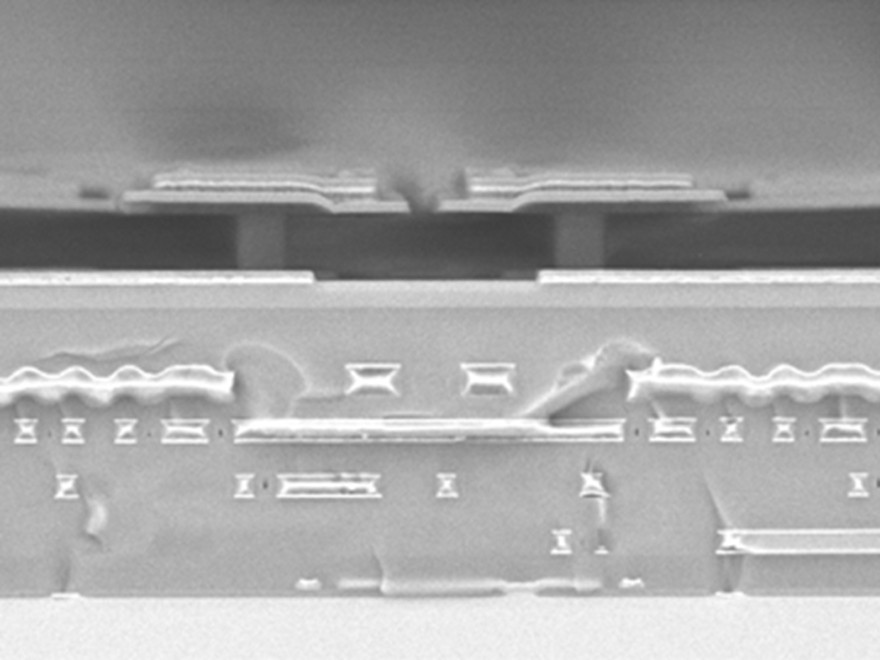
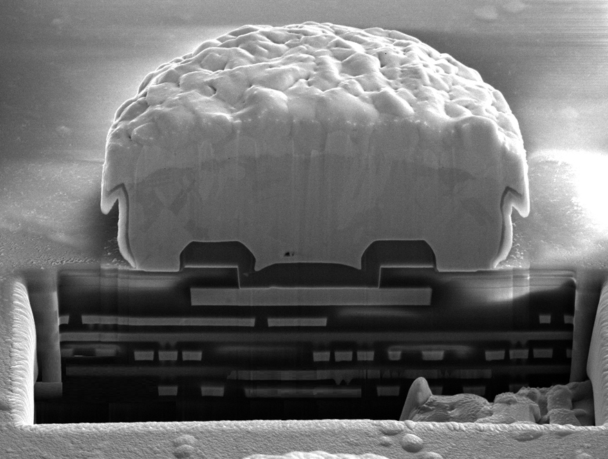
With its in-house clean rooms, the Fraunhofer IMS offers a wide variety of manufacturing processes for the realization of new technologies. Planarized CMOS surfaces serve as the basis for post-CMOS sensor integration. Furthermore, sensor elements such as optical, mechanical, physical, chemical and bio-sensors can be realized by combining them with "Micro-Electro-Mechanical Systems" MEMS or "Nano-Electro-Mechanical Systems" NEMS.
MEMS Technologies and Post-CMOS Processing


One example of customized MEMS technologies is post-CMOS processes for sensor integration. The fabrication of new devices using layer deposition and patterning is realized in the Microsystems Technology Lab&Fab (MST Lab&Fab). Sensors that can be realized with this principle are gas sensors, optical sensors, pressure sensors and also biosensors. If the sensor is then connected to a readout circuit by wafer-to-wafer bonding or C2W bonding, innovative and extremely compact microsystems are created for use in medicine, industry, mobility, space travel and security technology.
The Fraunhofer IMS offers the optimal technological infrastructure for the development and integration of innovative MEMS technologies. To continue the trend of compact and powerful devices in microtechnology ("More than Moore"), Fraunhofer IMS offers the possibility of 3D integration. By exploiting the third dimension, structures can be built on top of each other to achieve shorter interconnect paths and higher integration density. Furthermore, each plane can be manufactured in the optimal manufacturing process. This enormously increases the possibilities in the choice of technology, improves the yield and thus reduces the manufacturing costs. For this purpose, two powerful processes are available at the Fraunhofer IMS with the chip-to-wafer and wafer-to-wafer process. These processes are currently used in the manufacture of efficient and compact detectors consisting of optical backside illumination sensors and readout electronics. In the specific case of the wafer-to-wafer process, sensor and circuit wafers are precisely connected in the MST laboratory and electrically contacted via an ALD-optimized material stack. ALD technology can be used to produce not only electrical contacts but also protective layers, optical coatings, MEMS or NEMS devices for gas or biosensors with nanowires and ultra-thin free-standing membranes. Furthermore, Fraunhofer IMS realizes microbolometers as sensor elements of an uncooled infrared sensor on the CMOS wafer and is thus the only manufacturer of microbolometers in Germany.
Foundry services in the MST Lab&Fab
In addition to complete MEMS solutions, Fraunhofer IMS also offers foundry services in the Microsystems Lab&Fab. The clean room has lithography down to 0.35µm with the possibility to align back to front with 200 nm accuracy. In addition to standard coatings, coating thicknesses of up to 40 µm are possible, as well as colored coatings. Dedicated equipment can be used to bond fully integrated wafers (direct-wafer bonding) or individual circuits on wafers (chip-to-wafer-bonding). For plasma processes, sputtering (PVD), plasma-enhanced deposition (PE-CVD) and reactive etching (RIE) as well as deep etching (DRIE) are available. Further specialties here are the deposition of pure boron as ultra-thin passivation or contacting, silicon carbide, germanium as well as differently doped amorphous silicon. By means of electroplating, layers and structures up to 40 µm can be created from gold, copper, tin and nickel. Atomic Layer Deposition (ALD) is suitable as a highly conformal, biocompatible passivation as well as for many MEMS applications due to its excellent conformality. A variety of oxides and nitrides as well as metallic layers such as titanium nitride and ruthenium are possible here.
The above processes are all suitable for post-CMOS integration due to low process temperatures. Extensive characterization and analytics support the development and enable precise product controls. For this purpose, the MST Lab&Fab has a 3D microscope, an atomic force microscope (AFM), an electron microscope (SEM) with EDX, a scanning electron microscope for critical structures (CD-SEM), ellipsometers and profilometers.
Details about MEMS technologies at Fraunhofer IMS can be found in the links below.
