Customer benefits
- Customizable photonic platform
- Broad wavelength range
- Photonics and electronics on one chip
- Customizable material platform
- Low loss photonics
- Energy efficient circuits
- Photonic electronic integration
Our customizable photonics platform offers a broad wavelength range and is energy efficient thanks to (ultra-) low loss waveguides. The processes enable photonic – electronic integration on one chip.
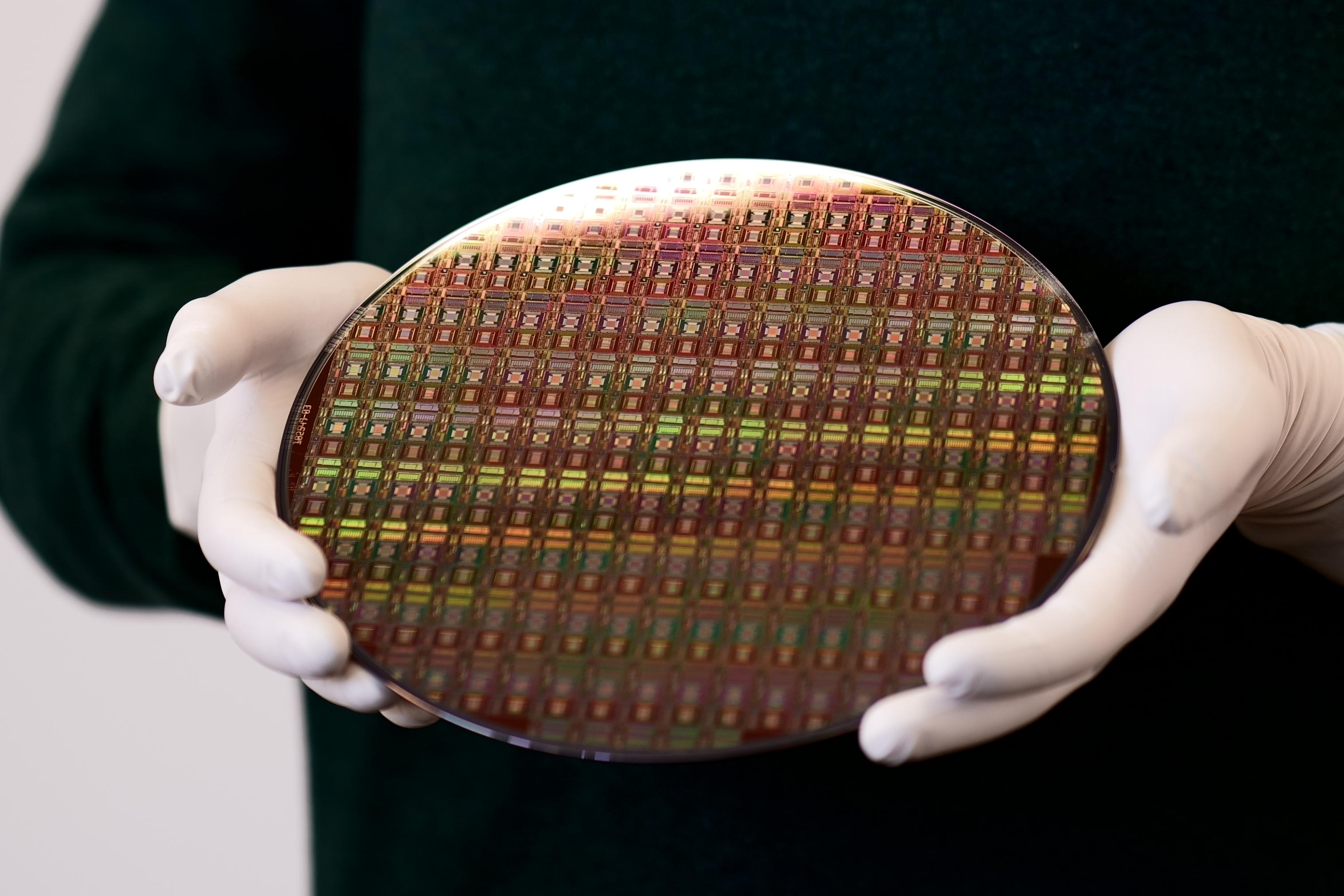
With our Photonic Integrated Circuit (PIC) technology, we offer cutting-edge solutions for a wide range of applications, such as sensing, photonic computing, and quantum technologies. Our post-CMOS compatible technology enables photonic integration on foundry wafers, making it possible to combine photonic and electronic components on one wafer. The photonic waveguides are manufactured on 200 mm wafers. Optionally, we also support process transfer and scaling.


We develop photonic circuits and systems based on dielectric materials. Our platform offers standard silicon nitride photonics, as well as processes for flexible integration of further materials to leverage their optical properties.
The Fraunhofer IMS photonic platform uses back-end-of-line processes to enable photonics as a post-processing option, which is especially useful for wafers with integrated electronics. In addition, we also provide post-processing for CMOS wafers from other foundries.
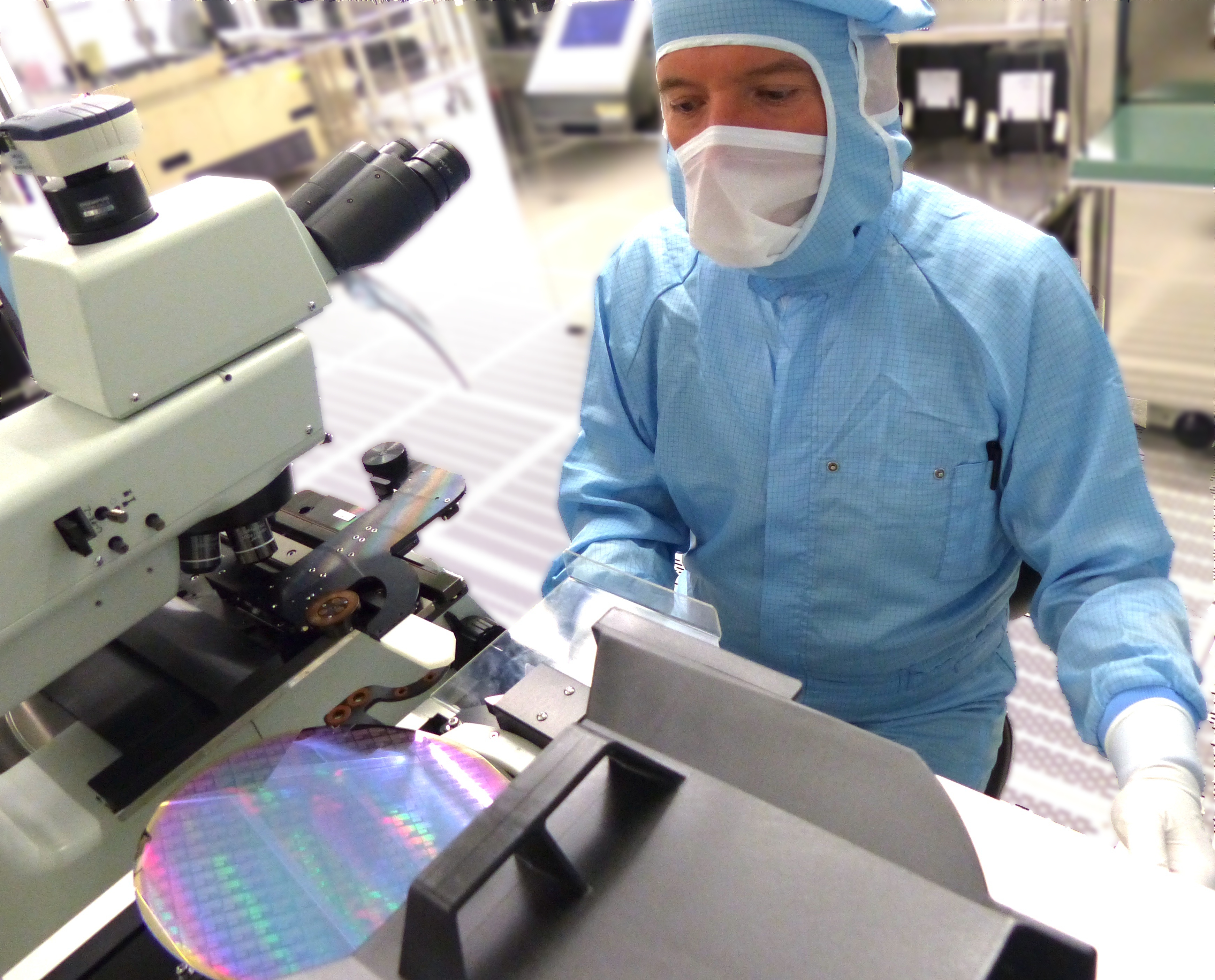
Our extensive experience in microelectronics manufacturing allows us to offer high-quality, reliable equipment manufactured at high yield rates in our state-of-the-art clean room facility.
Silicon nitride photonics offers low losses, no two-photon absorption and an extensive wavelength range from 400 nm to approximately 3 µm. Devices like couplers, waveguides, ring resonators, thermo-optical phase shifters, and more are available.
Integration and application of additional and new materials allow the implementation of exciting new functions. Other photonic materials, such as tantalum pentoxide and more, can also be used as waveguides.
The fabrication in our in-house clean room allows us to adapt process specifications, giving you the opportunity for application-specific designs. Dimension and material thicknesses can be custom tailored. We can also individually develop processes on your pre-processed wafers to adhere to your specifications fully.
Planarization options are available for heterogeneous integration of III-V semiconductor components. This opens the possibility of chip-to-chip or chip-to-wafer integration of laser sources and active elements.
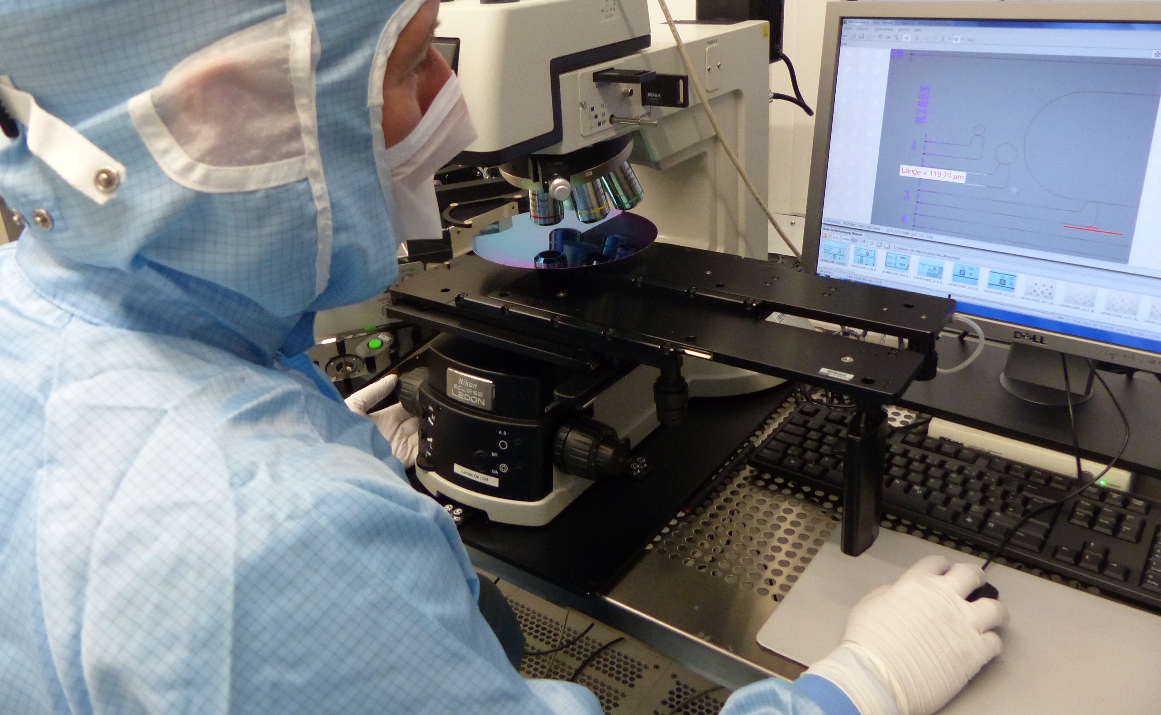
Our Fraunhofer IMS development team works closely with the photonics group of the Chair of Electronic Components and Circuits at the University of Duisburg-Essen. The focus is on the simulation of photonic components and the characterisation of the manufactured devices. Students and scientists can work at the forefront of research in integrated photonics. In research, we focus on integrated comb lasers and modulators with novel optoelectronic materials. Together with international partners, we solve more challenging integration aspects and can serve a wide range of applications.
We offer services in all steps from designing a product concept from your idea, all the way to pilot fabrication. Our services include:
Our technology platform is accessible via R&D collaborations and contracting. We are also open for collaborative projects with public funding.
