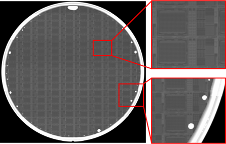
Deposition plays a central role in the fields of semiconductors, post-CMOS and micro- and nanoelectromechanical systems (MEMS and NEMS). Various deposition techniques are used to apply thin layers of different materials to substrates in order to achieve certain electrical, optical and chemical properties.
These processes are crucial for the development of modern electronics, from microprocessors to sensors. The layers can be made of different materials, including silicon, metals and insulators.
Chemical vapor deposition (CVD):
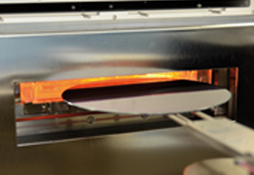
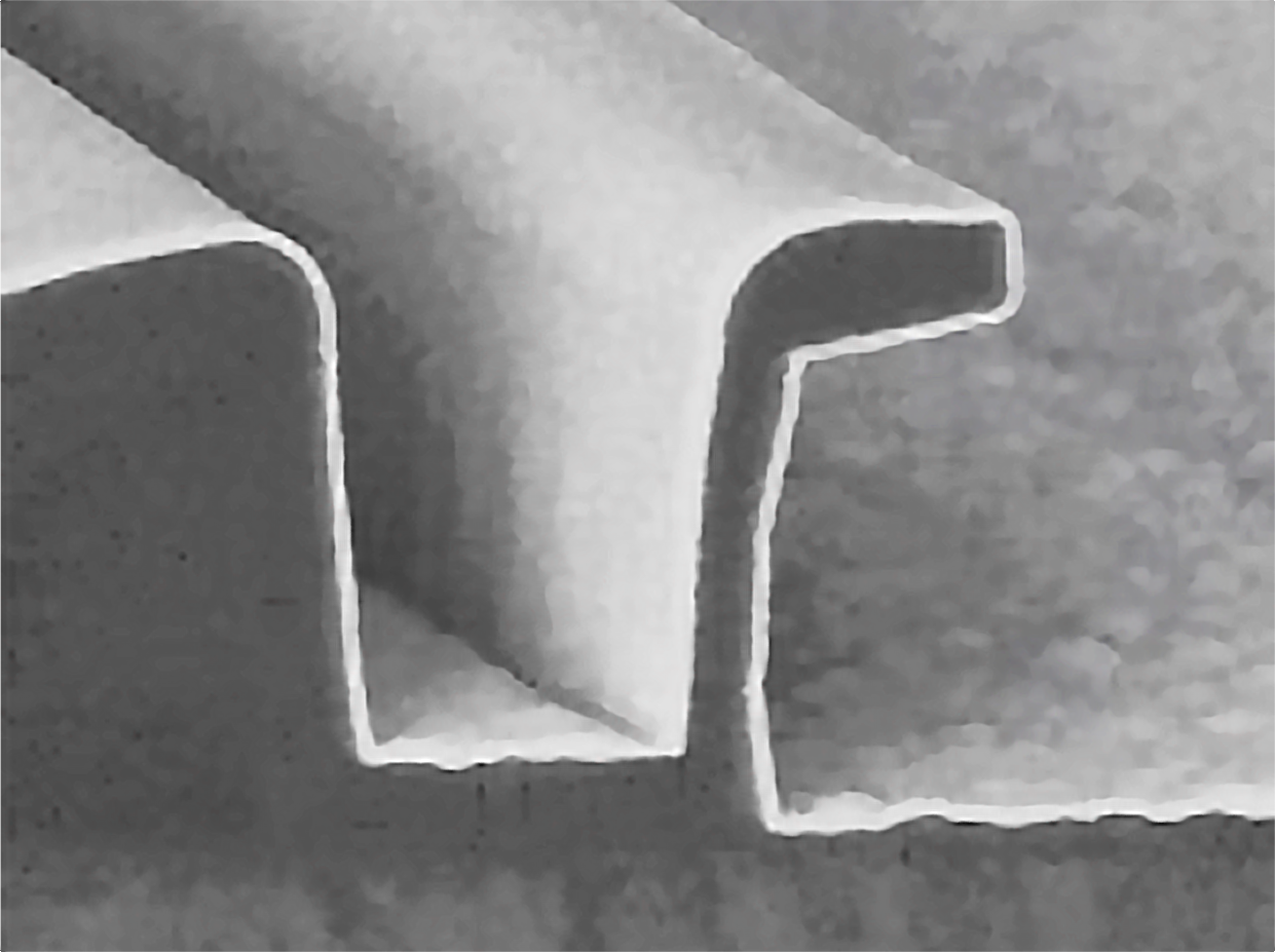
In this process, thin layers are deposited on a substrate by chemical reactions. One example is the deposition of silicon dioxide for insulation in integrated circuits. Another is the production of a conductive multilayer metallization by CVD with tungsten.
Low-pressure CVD (LPCVD):
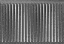
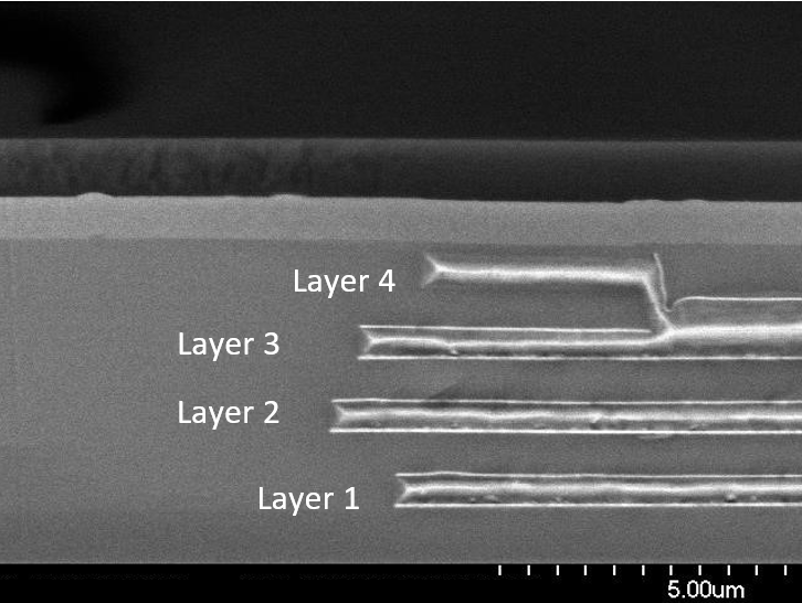
This variant of CVD is carried out under reduced pressure, which is ideal for conformal layers, e.g. SiN layers in our highly flexible platform for post-CMOS photonics.
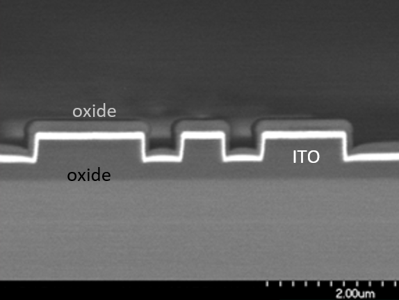
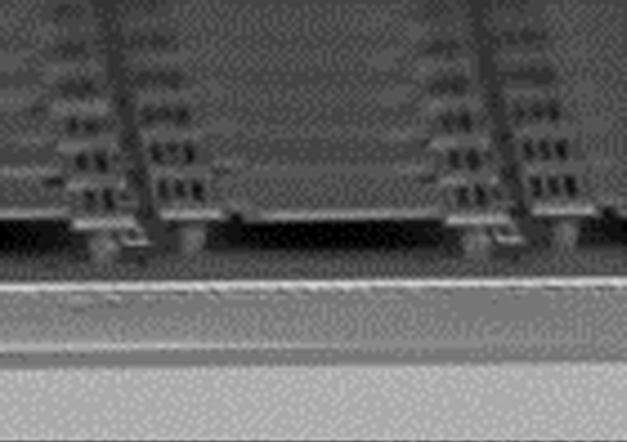
Atomic Layer Deposition (ALD):
ALD enables the precise deposition of atomically thin layers.
 Fraunhofer Institute for Microelectronic Circuits and Systems