
The IMS has been known for many years for its expertise in the manufacture of pressure sensors. The IMS develops application specific pressure sensors for medical applications, for different applications from low pressure/vacuum, over the barometric pressure range up to pressures of some 10 bar. The existing know-how covers different proven technological approaches for the fabrication of pressure sensors integrated in or integrated on CMOS circuits. In addition, the IMS has experience with silicon-on-insulator (SoI)-based technologies for the development of high-temperature pressure sensors. Both piezoresistive and capacitive sensor elements can be implemented for the electrical detection of the pressure variable.
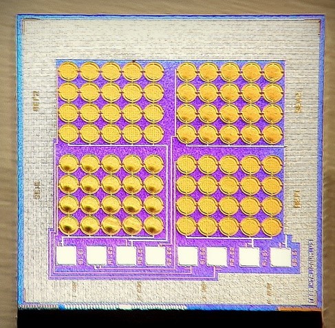
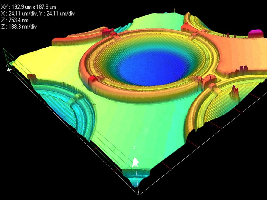
For the development of pressure sensor systems, several semiconductor manufacturing technologies based on 200 mm substrates (8" wafers) are available to the IMS. In addition to the CMOS production line for e.g. the high temperature pressure sensors, a Microsystems Technology (MST) Lab&Fab is also established at the Fraunhofer IMS. In this second clean room, so-called 1-chip systems are realized in which the pressure sensor elements, such as the pressure-sensitive membranes, are applied to the top of the existing ASIC by means of a post-CMOS process. This post-CMOS process is developed at Fraunhofer IMS and can be implemented in the MST-Lab&Fab.
The MST-Lab&Fab with its CMOS compatible infrastructure offers ideal conditions for the special requirements of process control on CMOS substrates, since a certain temperature budget must be maintained to guarantee the CMOS properties. This opens up the possibility of subsequently applying post-CMOS sensor elements to evaluation circuitry, which can be manufactured in external foundries using very high-performance CMOS technologies (e.g. 0.18 µm). Such System on Chip (SoC) solutions, which use the monolithic integration of MEMS on the CMOS IC to extend the functionality of ICs, are an attractive idea since the miniaturization of standard MEMS CMOS devices is limited. This monolithic integration method brings several advantages: The post-CMOS approach aims at reducing the geometry of MEMS sensors and increasing their functional range by freely choosing the CMOS technology. The post-CMOS approach allows flexible development of application-specific pressure sensor systems with the highest integration density. The sensor technology is decoupled from the CMOS technology. This offers the advantage that, for example, proven readout circuits can be used for different applications with different requirements for the pressure ranges, which can be manufactured cost-efficiently in proven technologies with very high throughput. At the same time, the sensor technology can be flexibly and efficiently adapted to individual pressure ranges with 6 to 7 process levels. By using ALD technologies, application-specific sealing and protection functions can be realized and it enables the use of pressure sensor systems of the IMS in different environmental conditions.
In a project running since 2018, the first generation of a CMOS chip in a 0.18µm technology has already been successfully developed as a readout chip for the post-CMOS production of pressure sensor elements. The design includes a high-resolution analog to digital converter (ADC) for digitizing capacitive pressure sensor signals. At the same time, the chip is extremely low-noise and suitable for use in transponder systems (LF or UHF). It can be connected to a large number of transponder chips available on the market via an SPI interface. Further development stages are possible. For example, one of the next development steps may be the integration of an interface for wireless communication (RF front-end). In the field of post-CMOS pressure sensor technology, we are looking for further partners for the development of application-specific pressure sensor systems with special requirements.
For more information, please visit our Infrastructure, Cooperation Models and Service & Know-How sections.
