Atomic Layer Deposition (ALD)-Technology

ALD is a deposition process based on the surface chemical reaction of at least two precursors. The process enables layer-by-layer growth of high-quality films with thicknesses in the range of 1-100 nm.

A steadily growing selection of ALD materials enables new innovative sensor applications. As a member institute of the Forschungsfabrik Mikroelektronik Deutschland (FMD) the Fraunhofer IMS acts as ALD competence center. ALD technology for 200 mm wafers is available at the Fraunhofer IMS.

© Fraunhofer IMS
© Fraunhofer IMS

You can benefit from these advantages:

  • Production of layers on substrates with complicated geometries and structures. The excellent side wall coverage of ALD layers in cavities with a high aspect ratio enables applications in the field of 3D technologies (e.g. DRAM).
  • Ultra-thin layers with a layer thickness accuracy at the Ångström level
  • The deposited ultra-thin layers are of high quality, high density and almost free of pinholes. This makes it possible to use them as hermetic protective layers for implants of various kinds.
  • Customized process development for your application. We offer you maximum flexibility to develop processes on whole wafers (up to 200 mm), on chip level and on other 3D objects.
  • We perform precursor screenings to find a suitable ALD precursor for your application. In cooperation with our partners, suitable ALD precursors can also be developed.
  • A growing variety of materials is available: metals, oxides, sulfides and nitrides, 2D materials, as well as inorganic-organic hybrid materials are provided by Fraunhofer IMS.
  • Scalable processes from single wafers to batch coating

You benefit from these established materials for your application

Material

Temperature Range

Applications

Al2O3

50 °C - 300 °C

Dielectric oxide

HfO2

200 °C – 300 °C

High-k dielectric

ZrO2

200 °C – 300 °C

High-k dielectric

Ta2O5

100 °C - 250 °C 

Biocompatible Encapsulation

TiO2

100 °C

Biocompatible encapsulation

ZnO

80 °C - 250 °C

Sensor Material

ZnO:Al

150 °C

Transparent conductive oxide

SnO2


100 °C – 200 °C Sensor material
TiAlCN 380 °C - 400 °C Conductor, thermal barrier
TiN 300 °C - 400 °C Conductor, adheasion promoter
LiPON 300 °C Solid state electrolyte
Ru 300 °C - 325 °C Metallic conductor
MoS2 100 °C  2D-TMDC semiconductor
WS2 300 °C - 350 °C 2D-TMDC semiconductor
TiO2 / Al2O3 100 °C Biomedical encapsulation
HfO2 / Al2O3 200 °C Biomedical encapsulation
ZrO2 / Al2O3 200 °C Biomedical encapsulation
Ta2O5 / Al2O3 100 °C Biomedical encapsulation

You can benefit from these ALD IMS specialties:

© Fraunhofer IMS

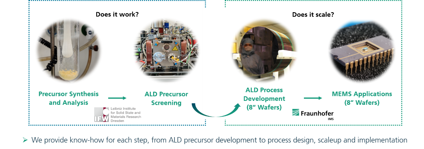
Since the process temperature during ALD deposition is low compared to conventional CVD processes, ALD layers can be deposited particularly well on substrates with integrated circuits, i.e. on CMOS wafers. Thus, ALD technology can be used for various MEMS, NEMS or CMOS-related applications, such as:

  • Development of new precursors, processes and materials for molecular sensors, e.g. chemiresistive gas sensors and biosensors with a focus on transition metal dichalcogenides (2D-TMDC) materials such as MoS2 and WS2
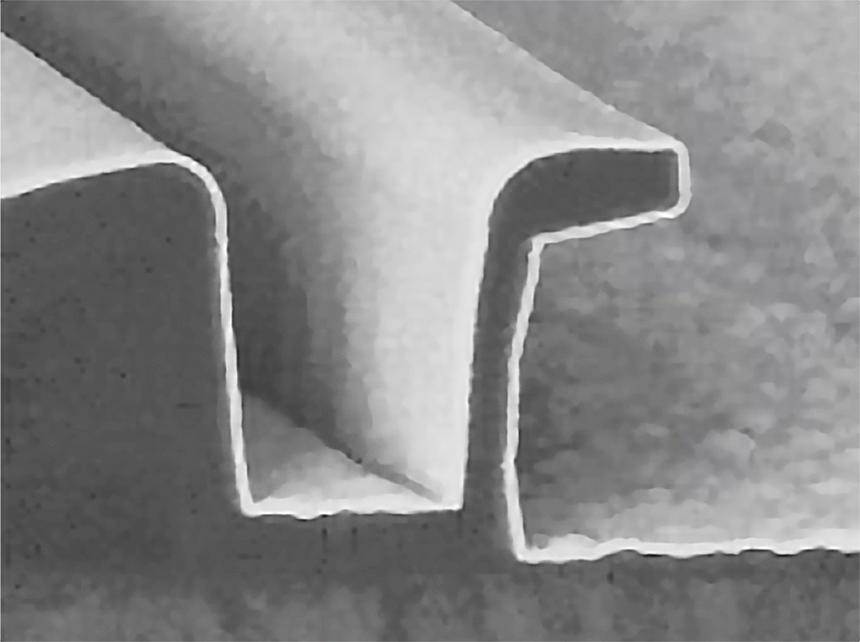
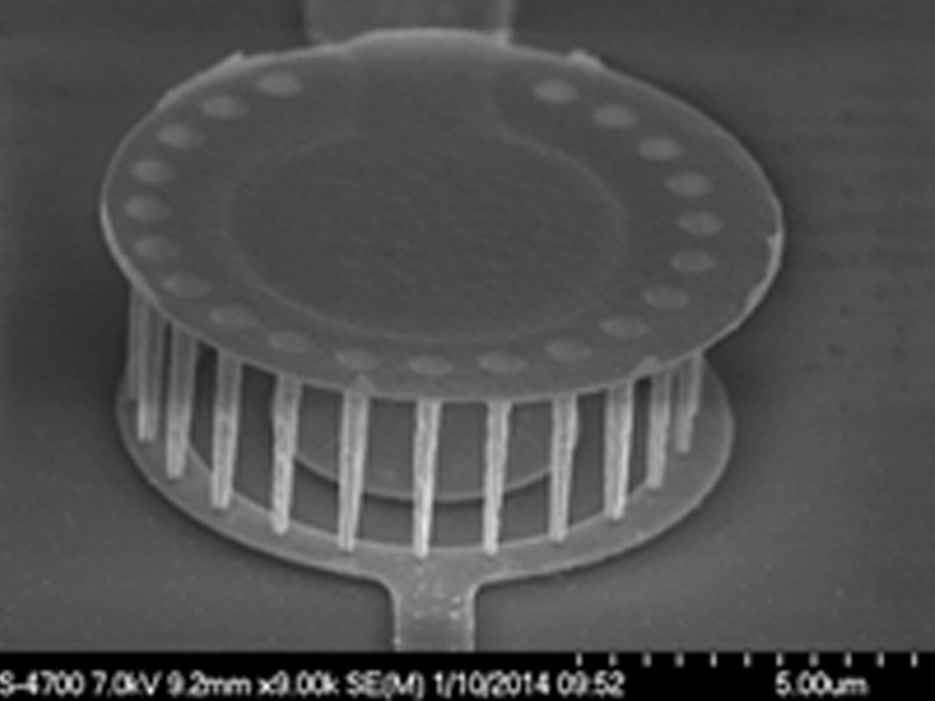
  • Cost-effective 3D-NEMS technologies for the generation of free-standing nanostructures on CMOS surfaces with the highest reproducibility have been developed and patented by the Fraunhofer IMS.
  • Media-resistant layers for sensor applications such as pressure sensors or for the encapsulation of medical implants. Nanolaminates are available as ALD passivation. Further ALD materials can be implemented at the Fraunhofer IMS upon request.
  • Electrical or optical shielding can be produced by metallic layers such as ruthenium (Ru). Furthermore, ALD layers can be used as transparent conductive electrode layers, for example for optical sensors or solar cell applications.

Our technologies - Innovations for your products

3D Integration

3D integration using wafer-to-wafer bonding (W2W) and chip-to-wafer bonding (C2W) enables cost reduction through higher integration density and shorter interconnect distance.

Microbolometer

Technology process for the production of customized uncooled infrared sensors for applications in the wavelength range 3 µm to 5 µm or 8 µm to 14 µm.

Vacuum Chip-Scale-Package

We have implemented the smallest possible vacuum package for uncooled IR imagers using vacuum chip scale packages (CSP) technology.

Pressure Sensors

We operate processes for the manufacture of pressure sensor systems in both CMOS and MST production lines.

SPAD in focus

Highly sensitive image sensors with adapted microlens arrays 


Technology (Home)

Here you can get back to the overview page of the core competence Technology.