Development of CMOS and customized CMOS compatible processes

Experience in the field of CMOS technology development at Fraunhofer IMS

For more than 35 years, Fraunhofer IMS has been engaged in CMOS technology developments and has as its development base a 200 mm CMOS line according to industrial standards with various robust CMOS processes down to a minimum structure size of 0.35µm (Center for Sensor Technology).

The Fraunhofer IMS optimizes CMOS processes in the sense of the "More-than-Moore" principle by integrating additional functions such as high-voltage-resistant components, high-frequency circuits and sensors. Fraunhofer IMS also develops technologies that allow the use of the circuit under harsh conditions.

The preparation of CMOS wafers as "smart" substrates by e.g. planarization is also an important development task. On these "intelligent substrates" layers are deposited and patterned by post-CMOS processes and thus new, additional components are realized on the CMOS circuits.

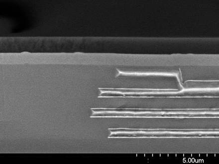
SEM cross section of the 4 metal layers of the 0.35µm automotive CMOS
© Fraunhofer IMS
SEM cross section of the 4 metal layers of the 0.35µm automotive CMOS

Development of application and customer-specific CMOS processes

Examples for the complete development of customer and application specific CMOS processes are the development of a mixed signal 0.35 µm automotive CMOS process as well as the development of high temperature electronics (300 °C) and high voltage SOI CMOS (1200 V) processes.

In this context, accompanying process and component simulations (TCAD) as well as electrical characterization including parameter extraction and reliability investigations are part of the Fraunhofer IMS activities.

The integration of special components and process modules into our own or customer CMOS processes is also an important field of activity.

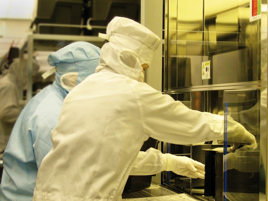
CMOS Line according to industrial standard
© Fraunhofer IMS
CMOS Line according to industrial standard

This applies, for example, to sensor technology in the form of optically sensitive components such as SPADs (Single-Photon Avalanche Diodes) as well as pressure sensores.

But also other circuit components such as non-volatile memories (EEPROM or flash cells) including specific circuit development, as well as high voltage components are a field of activity in which we have a lot of experience. Special process modules for UV-transparent passivation and the removal of dielectric layers over a photodiode with subsequent deposition of an anti-reflective coating are also part of the Fraunhofer IMS repertoire.

In addition to the integration into the CMOS process, Fraunhofer IMS is also engaged in the development of CMOS compatible processes for discrete devices such as SiPM and DEPFET, which also include the development of appropriate interconnect technologies, such as double-sided wafer processing.

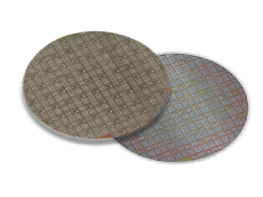
Front and back side for double-sided wafer processing
© Fraunhofer IMS
Front and back side for double-sided wafer processing

Post CMOS Process for sensor integration

Planarized CMOS surfaces serve as the basis for post-CMOS sensor integration.

By combining them with "Micro-Electro-Mechanical Systems" MEMS or "Nano-Electro-Mechanical Systems" NEMS, sensor elements such as optical, mechanical, physical, chemical and bio-sensors can also be realized. Examples of this are uncooled bolometer arrays as well as nanowire gas sensors. The combination of CMOS and MEMS (or NEMS) creates innovative and extremely compact microsystems for use in health, industry, mobility, through to aerospace and security applications.


Atomic Layer Deposition (ALD)

State-of-the-art ALD processes for innovative sensor technology ALD-Catalyt for new MEMS/NEMS Devices.


MEMS for Harsh Environments

Optical MEMS for harsh environments are typically needed for specific application fields such as oil exploration, chemical industry and the aerospace or automotive sector.

Services and Know-How around Silicon

Fraunhofer IMS is your professional partner throughout the development of process steps, process modules and complete micro/nano sensor systems.

Microsystems Technology Lab&Fab

We provide intelligent post processing in our Microsystems Lab&Fab.

Devices & Technologies

Our services covert he whole range from providing single process steps to customer orientated technology and device development, qualification, and pilot fabrication.

Our technologies - Innovations for your products

High Temperature Technology

The high-temperature technology of the Fraunhofer IMS allows integrated circuits to operate at temperatures up to 300 °C operating temperature.

External technology development

Fraunhofer IMS develops technologies according to customer specifications or extends already existing technologies with customer options.

Our technology areas - Our technologies for your development

Image Sensors

Development of individual sub-steps up to the complete customer-specific process.

MEMS Technologies

Low temperature processes for post-CMOS integration of MEMS sensors or actuators.


Biofunctional Sensors

Tools for medical diagnostics.


Technology (Home)

Here you can get back to the overview page of the core competence Technology.