

An important parameter of image sensors with a decisive influence on sensitivity is the fill factor. This describes the proportion of the light-sensitive area to the total area and thus the proportion of incident photons that can be detected. Especially SPAD (Single-Photon Avalanche Diode) - based sensors usually contain very complex electronic circuits within the pixels, which limit the light-sensitive area and thus the fill factor. By vertically arranging active sensor elements and the circuitry (3D integration) an improvement can already be achieved, yet the pixel size is still determined by the size of the readout circuit.
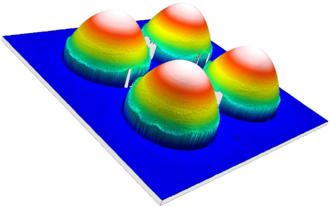
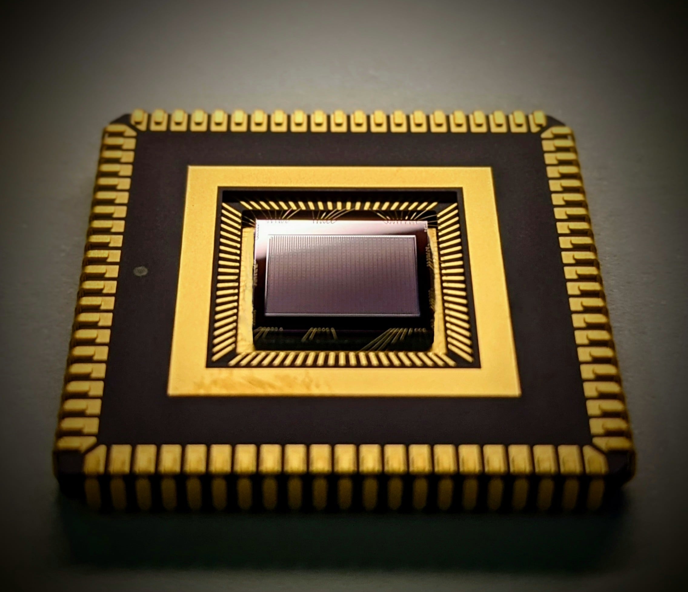
Microlenses that focus photons onto the light-sensitive areas of the sensor can overcome this limitation and thus bring about a decisive increase in performance. As part of the Fraunhofer-internal project "SPAD im Fokus", in cooperation with the Fraunhofer Institute for Applied Optics and Precision Engineering (IOF). Customized microlens arrays for the 32 x 24 pixel CSPAD αlpha sensor were applied and significantly increase the effective fill factor. Based on the sensor architecture, an optimized lens design was created and simulated for this purpose. Using photolithography and reflow of photoresist, the microlens arrays adapted to the CSPAD αlpha-wafer layout were mastered at wafer scale and then transferred to a replication tool. In the molding process, liquid polymer is applied to the sensor wafer and formed into the desired shape using the replication tool. Selective curing with UV light allows the areas outside the active sensor area to be kept free of polymer.
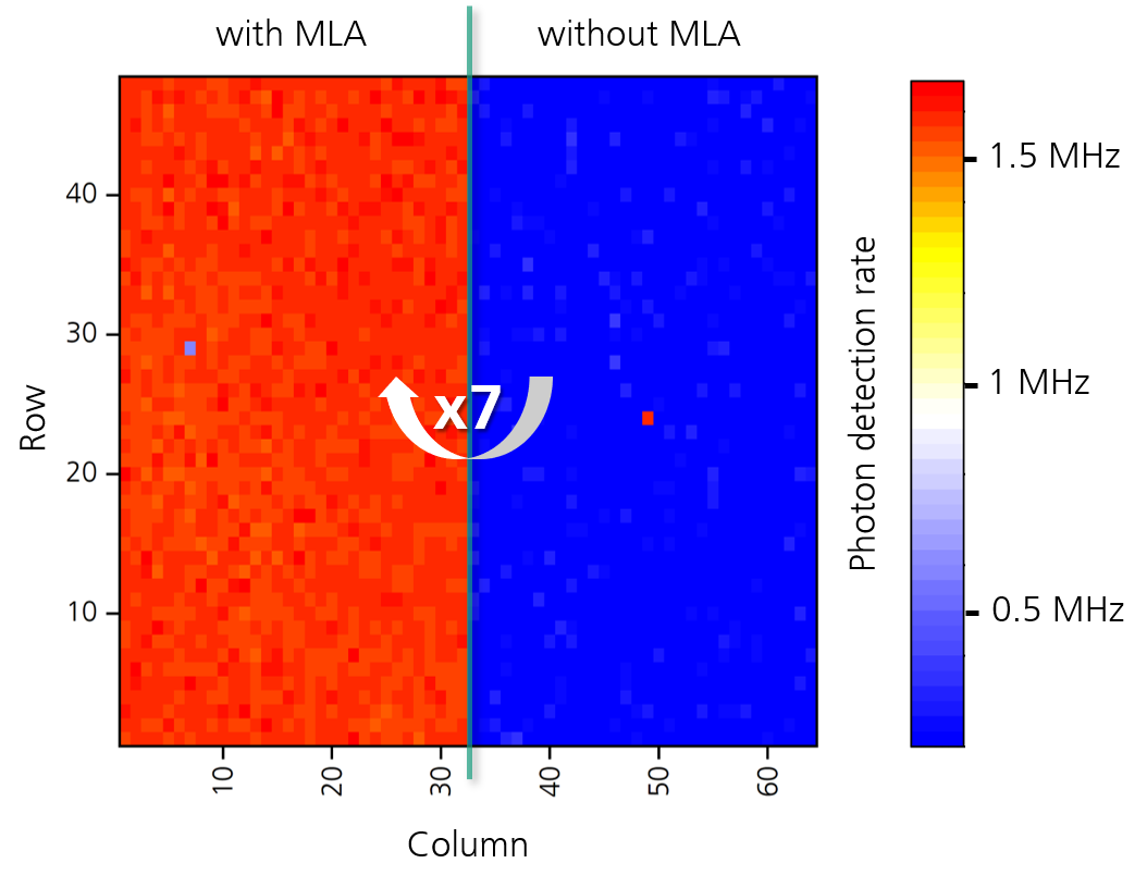
The sensors can then be separated, assembled into a package and operated regularly. Electro-optical characterization by homogeneous defined irradiation shows an increase in photon detection efficiency by a factor of 7. Accordingly, the lenses capture and focus a 7-fold higher number of photons onto the light-sensitive areas of the SPADs without any negative influence on the sensor. Due to the possibility of replication on wafer level, high numbers of sensors can be equipped with microlens arrays and significantly improved by this method at low cost. The combination of the highly sensitive SPAD sensor device and the increased sensitivity provided by matched microlens arrays enables high-performance single-photon detection for imaging applications such as LiDAR and quantum imaging.
Additional information on the Fraunhofer IMS 3D Sensors based on the CSPAD technology can be found here.
Fraunhofer IMS is continuously working on the development and optimization of SPAD-based sensors and is looking for partners for applications of this technology. Please feel free to contact us!
