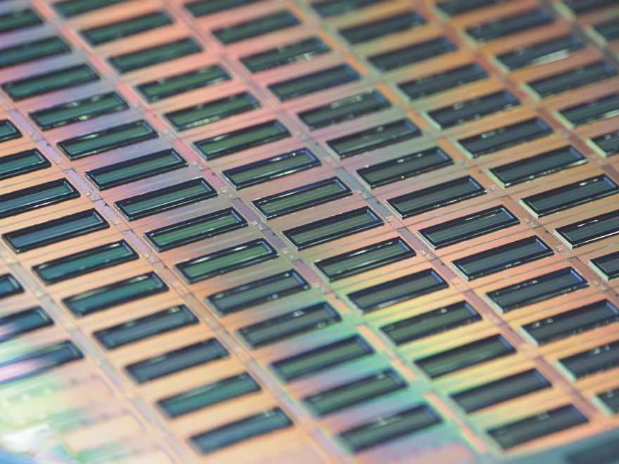
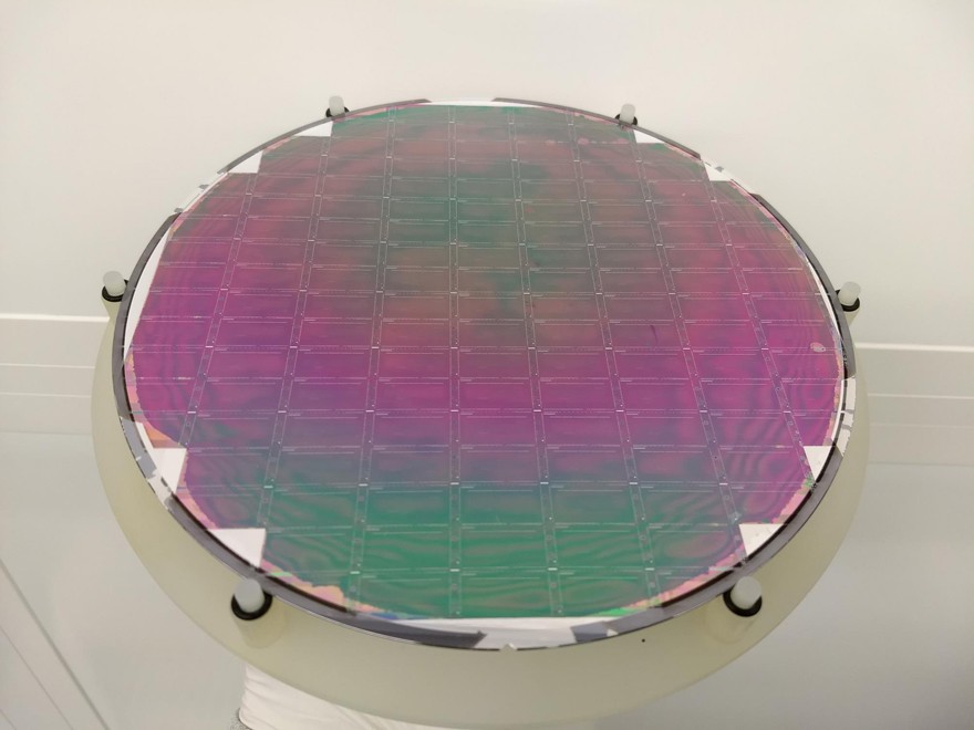
By exploiting the third dimension and the possibility of heterogeneous integration, structures from different process lines can be combined. For example, 3D integration allows optical sensors to be bonded directly to the associated interpreting and signal processing circuit logic. As current new developments place ever higher demands on the detectors, it is increasingly necessary to manufacture the detectors in specialized technologies and to produce the signal-processing circuit parts in a technology with very small structures. This allows, for example, the interpretive readout circuit to be outsourced to the third dimension and the optically active area to be enlarged, thus significantly increasing sensitivity.
Fraunhofer IMS supports different technologies for 3D integration on 200 mm wafers.
Wafer-to-Wafer-Bonding
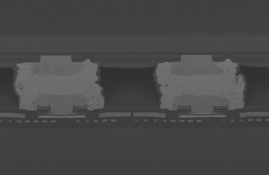
Fraunhofer IMS has a direct oxide-to-oxide bonding process for 3D integration, which is performed at CMOS-compatible temperatures below 400 °C. Direct wafer bonding is based on the formation of covalent siloxane (Si-O-Si) bonds. For this purpose, the wafer surfaces are activated in oxygen plasma to generate silanol (Si-OH) groups under an H2O atmosphere. The wafers are aligned and contacted to each other so that hydrogen bonds are formed in the bond interface region. Finally, the pair of wafers is heated to over 250 °C and strong covalent siloxane bonds are formed by the diffusion of water away. To produce a high-quality bond, the following surface properties must be taken into account:
Topology, Microroughness, Bending, Particle contamination
Based on many years of experience at Fraunhofer IMS in CMOS and MEMS processes as well as in packaging technology, optimized stress compensation and chemical mechanical planarization (CMP) processes as well as adapted layout designs for W2W bonding could be developed. With the process optimizations, a shear strength of more than 4 kg/mm2 and a precision accuracy of the wafer bond of less than 2 µm are achieved.
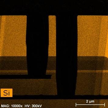
The front-side silicon through-silicon vias (TSV) are filled with an ALD (Atomic Layer Deposition) optimized material stack. Different µVia variants allow the process to be adapted to individual customer design specifications.


