Services & Know-How in the Field of Devices and Technologies

Development and integration of innovative microelectronic and micromechanical devices and systems

Use our services and the know-how of the Fraunhofer IMS in the fields CMOS and microsystems technology for the development of innovative and compact microsystems.

The Fraunhofer IMS can rely on 30 years of experience in the area of CMOS technology development and has been focusing especially following areas:

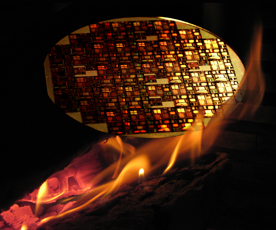
Hochtemperatur-ICS auf Basis der SOI-CMOS-Technologie für den Temperaturbereich von -50 °C bis 300 °C
© Fraunhofer IMS
Hochtemperatur-ICS auf Basis der SOI-CMOS-Technologie für den Temperaturbereich von -50 °C bis 300 °C

CMOS

 
  • Development and transfer of process modules  for CMOS, e. g. non-volatile memory, analog devices, optical devices and voltage-proof devices
  • Development of CMOS technologies, for example high-temperature SOI-CMOS technologies on the basis of integrated circuits for the application for application in up to 300 °C
  • Realization of extra steps, e. g. surface planarization
  • Production of pilot series in the clean room

In addition to the field CMOS, Fraunhofer IMS has the microsystems technology Lab&Fab available and can offer the following services and know-how:

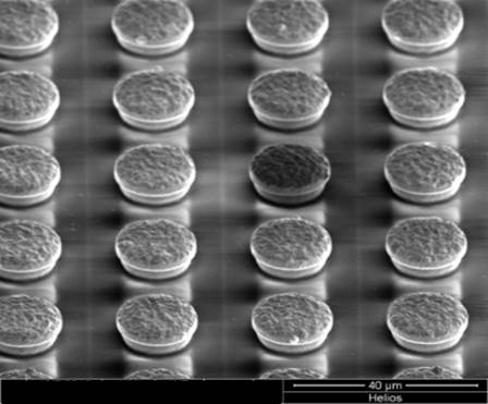
REM-Aufnahme von Cu/Sn-SLID-Bumps zur Kontaktierung im Chip-zu-Wafer-Verfahren
© Fraunhofer IMS
REM-Aufnahme von Cu/Sn-SLID-Bumps zur Kontaktierung im Chip-zu-Wafer-Verfahren

MST process steps

  • Deposition and structuring of layers:
  • Chemical vapor deposition (CVD) of amorphuous Si, SiO2, Si3N4, SiGe, Ge, SiC, Diamond like  Carbon (DLC)
  • Atomic layer deposition (ALD) of Al2O3 , Ta2O5 , Ru, TiAlCN, TiN, ZnO
  • Physical layer deposition of metals, for example Ti, TiN, TiW, AlSi, Cu
  • Electroplating of Cu, Sn, Ni, Au
  • Lithography with precise wafer back-to-front side alignment
  • Etching processes: ICP, RIE, DRIE, Si deep etching, wet etching
  • 3D integration using wafer-to-wafer and chip-to-wafer connections:
    • Direct wafer bonding
    • Solid-liquid interdiffusion bonding (SLID)

Through the combination of CMOS and MEMS processes expertise, Fraunhofer IMS can offer different 3D integration technologies:

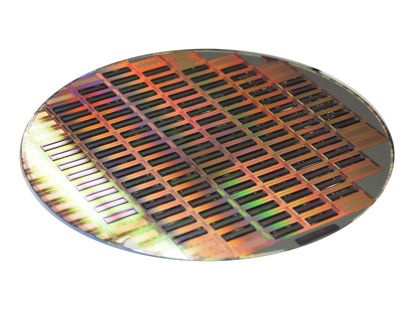
Fully equipped wafer using chip-to-wafer process
© Fraunhofer IMS
Fully equipped wafer using chip-to-wafer process

MEMS on CMOS

  • 3D-Integration of MEMS and CMOS devices or circuits for MEMS-based systems
  • Sensor processes
    • Optical detectors
    • Microbolometer arrays for far-infrared sensors
    • Pressure sensors in surface micromechanics
    • Color filters and microlenses for optical devices
    • Optical special devices
    • Biosensor elements
  • Production of pilot series in Fraunhofer IMS CMOS and MST clean rooms  

This might interest you

Infrastructure

Learn more about our infrastructure for the production of microelectronic and micromechanical devices and systems.

Cooperation Models

The Fraunhofer IMS offers cooperation models in the fields of devices and technologies from the conception phase to pilot series production.  

Overview Pages

Devices and Technologies (Home)

Fraunhofer IMS offers the optimal conditions for the development of innovative microelectronic and micromechanic devices and systems.

Applications

Overview of typical development projects in the field of Devices and Technologies

Technologies

Customer-specific CMOS process, high-temperature ICs, MEMS and post-CMOS processing, atomic layer deposition (ALD), 3D-Integration

Customer Benefits

Our offers for customer-oriented solutions – from the process development up series production

Download