3D-Integration in the field of microelectronics

The Fraunhofer IMS offers various technologies for 3D-Integration in order to continue the trend of microelectronics: faster, more compact and more powerful

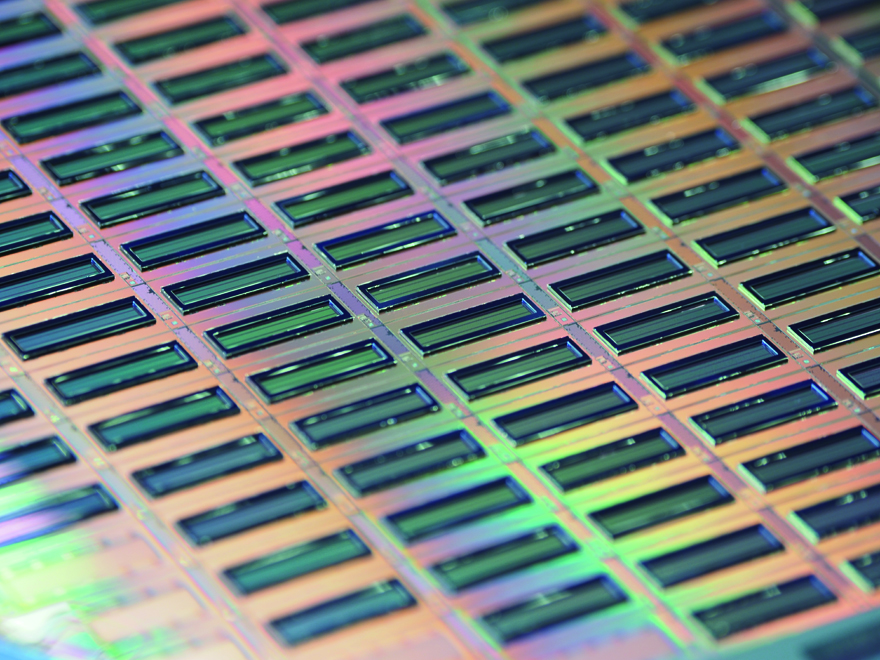
8““-wafers with fitted detector chips, manufactured by chip-to-wafer process
© Fraunhofer IMS
3D-Integration of detector chips with signal-processing circuit logic using SLID bonding techniques
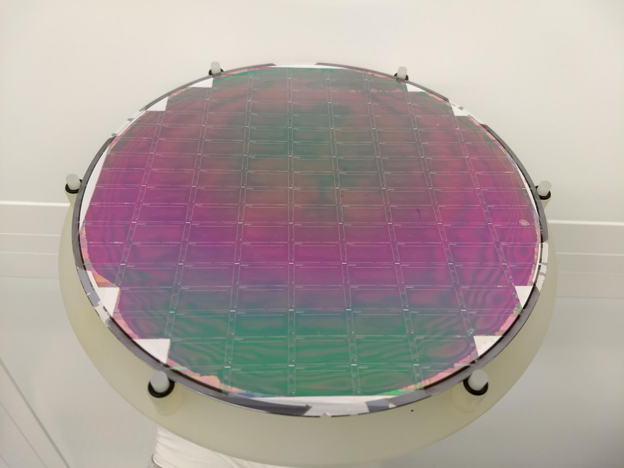
Wafer bond consisting of sensor and circuit wafer before post-prosessing
© Fraunhofer IMS
Wafer bond consisting of sensor and circuit wafer before post-processing

In recent decades, research and development in the field of micro- and nano- electronics has led to ever smaller structural sizes and continuously increasing integration densities of sensors, memories and processing circuits. Due to the physical limitation, the enormous technological growth regarding a wafer level is stagnating. 

The 3D-Integration of micro- and nano-electric construction elements allows a vertical arrangement of different system devices and offers a way to continue the trend of compact and powerful devices (“More than Moore”)

3D-Integration offers further advantages:

  • Cost reduction
  • Shorter connecting paths
  • Higher integration density

By exploiting the third dimension and the possibility of heterogeneous integration, structures from different process lines can be combined with a heterogeneous integration. Through 3D-Integration, e. g. optical sensors can be manufactured directly with the associated interpreting and signal processing circuit logic. Since current new developments place ever higher demands on the detectors, it is increasingly necessary to manufacture the detectors directly with the signal-processing circuit logic. Thus, for example, the interpreting circuit can be moved into the third dimension in order to increase the optically active area and thus the sensitivity.

Fraunhofer IMS supports various technologies for 3D-Integration on 200 mm-wafers.

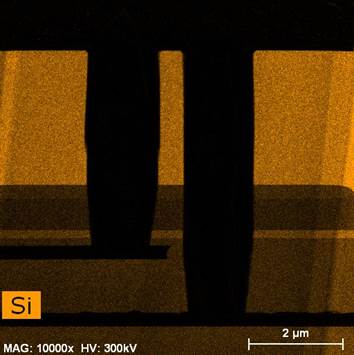
Representation of etched µVia structures for front-side silicon through-plating
© Fraunhofer IMS
µVia-structures for front-side silicon through-hole plating in wafer-to-wafer bonding

Wafer-to-Wafer-Bonding (W2W)

The Fraunhofer IMS offers a direct oxide-to-oxide bonding processfor 3D-Integration at CMOS compatible temperatures below 400 °C. The bonding process is based on the formation of covalent siloxane (Si-O-Si) compounds. For this purpose, the wafer surfaces were activated in the oxygen plasma to generate silanol (Si-OH) groups under an H2O atmosphere. The wafers are aligned to each other and conducted so that hydrogen bonds are formed in the area of the bond interface. Finally, the pair of wafers is heated to over 250 °C to created covalent siloxane compoundsby diffusion of water. The following surface properties must be observed in order to produce a high-quality bond:

  • Topology
  • Microroughness
  • Bend
  • Particle contamination

Through many years of experience at the Fraunhofer IMS in CMOS and MEMS processes as well as in assembly and interconnection technology, optimized stress compensation and chemical mechanical planarization (CMP) methods as well as adapted layout designs for W2W-bonding could be developed with many years of experience in CMOS/MEMS processes, assembly and interconnection technologies. With these process optimizations, a shear strength of over 4 kg/mm2 and a precision accuracy of the wafer bond of less than 7 µm can be achieved. The front side interconnection (TSV, Through Silicon Vias) is realized through µVias, filled with an optimized ALD (Atomic Layer Deposition) material stack. The process can be adapted to individual customer design specifications by different µVia variants.

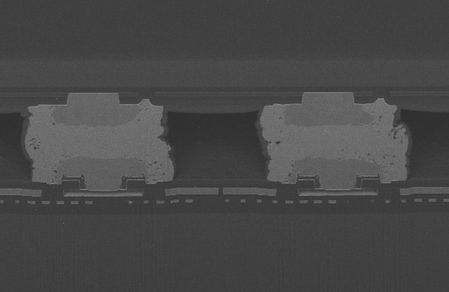
Cu/Sn-Microbumps for contacting via SLID process
© Fraunhofer IMS
Cu/Sn-Microbumps for contacting via SLID process

Chip-to-Wafer-Bonding (C2W)

The Fraunhofer IMS offers chip-to-wafer bonding with an solid-liquid interdiffusion (SLID) process. The SLID bonding is based on an two-metal-system to create high-temperature stable contacts at a low process temperatures.  For this purpose, a low-melting metal is brought into contact with a suitable metal partner with a higher melting temperature and then melted.Diffusion processes occur at the interfaces and an intermetallic phase is formed. Depending on the material combination, contacts with a temperature stability from 400 °C up to 600 °C can be produced.  

The Fraunhofer IMS uses the flip-chip method for 3D-Integration. For the assembling process, the chip is soldered onto the wafer with the active surface facing downwards. The chip size can vary from only a few mm to the µm range. The contacting is made by micro bumps, which are aligned with high precision (precision accuracy < 5 µm). The bump size ranges from a few µm to 100 µm. The Fraunhofer IMS offers galvanic deposition of the following materials for the production of micro bumps:

  • Copper (Cu)
  • Tin (Sn)
  • Gold (Au)
  • Nickel (Ni)

Based on many years of process experience, the CuSn and Ni/Au/Sn-SLID bonding processes are established at the Fraunhofer IMS. The manufactured CuSn and Ni/Au/Sn bump contacts are stable at temperatures up to 675 °C and 522 °C respectively and withstand over 1000 temperature cycles (-55 °C to 150 °C).

With the wafer-to-wafer and chip-to-wafer bonding,  we have two strong and established process for 3D-Integration at your disposal.

This might interest you

Customer-specific CMOS processes

Development from a single sup step to the complete customer specific CMOS process

Atomic Layer Deposition (ALD)

State-of-the-art ALD processes for innovative sensor technology.

MEMS Technologies

Low temperature processes for post-CMOS integration of MEMS sensors or actuators

High Temperature Electronics

At Fraunhofer IMS we develop integrated circuits, sensors and actuators in a 0.35 µm SOI-CMOS high temperature technology and manufacture them in our in-house clean room.

Overview Pages

Devices and Technologies (Home)

Fraunhofer IMS offers the optimal conditions for the development of innovative microelectronic and micromechanic devices and systems.

Applications

Overview of typical development projects in the field of Devices and Technologies

Technologies

Customer-specific CMOS process, high-temperature ICs, MEMS and post-CMOS processing, atomic layer deposition (ALD), 3D-Integration

Customer Benefits

Our offers for customer-oriented solutions – from the process development up series production

Download