3D-Sensing

Stereoscopic vision and sophisticated data processing in the brain enables humans to sense their environment in three dimensions. An increasing number of emerging technologies also demands this 3D-Sensing capability from machines and systems, often with stringent requirements for the safety and reliability of each method.

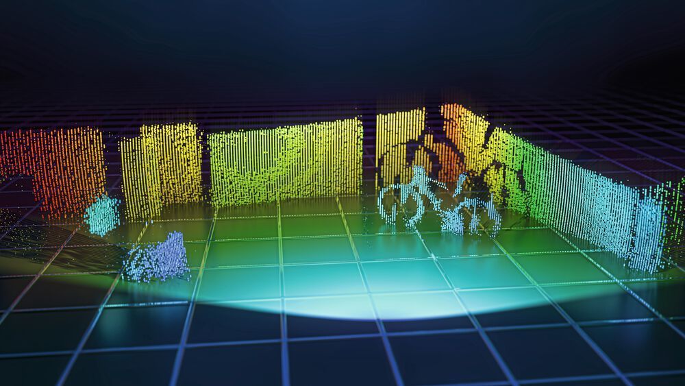
A popular and proven approach to 3D-Sensing, the 3-dimensional detection of the environment, is distance determination by measuring the time of flight of light, the time-of-flight (ToF) method. Here, a laser pulse is emitted, reflected by an object and then detected on an image sensor. The distance of the object can be determined from the duration of the time of flight and the speed of light. As LiDAR (from Light Detection and Ranging), this method is already frequently used, for example, in driver assistance systems, smartphones and robotics. More about this application in the field of "autonomous driving" can be found here.

The advanced development of lasers and the high speed of light allow in principle very fast distance determination and thus 3D-Sensing in real time. However, this places very high demands on the image sensor used, which must have the ability to reliably detect photons while determining the time of arrival with high resolution. In addition, if the distances of different points in space are to be determined, multiple pixels with independent time-determining elements are required on the image sensor.

Especially when LiDAR is used in autonomous vehicles, there are additional challenges, such as the background light of the sun, which can vary greatly and must still be distinguished from the laser light, which pose additional challenges to the image sensor. Since the transmitter (laser) side is largely limited here by the eye safety requirement, the main focus is on optimizing the receiver (image sensor) and subsequent data processing.
CMOS wafer with the image sensor CSPAD αlpha
© Fraunhofer IMS
Using the in-house CMOS process, the SPAD sensor elements and evaluation electronics can be manufactured directly together.

Expertise

The CSPAD sensors developed by Fraunhofer IMS combine highly sensitive 3D sensing capabilities with secure algorithms for high-performance use in LiDAR applications, among others. The central goal is to achieve maximum range even at high sunlight intensity and low system costs at the same time. Apart from the typical application area LiDAR, CSPAD sensors can also be used in other fields requiring time-resolved detection of photons like spectroscopy, quantum imaging and random number generation, among others.

The CSPAD technology is based on the integration of SPADs (Single-Photon Avalanche Diodes) in a 0.35 µm CMOS process certified for the automotive industry and optimized for optoelectronic applications. This allows SPAD sensor elements and read-out electronics to be accommodated on the same chip.  In addition, backside-illuminated CSPAD sensors can be realized using 3D integration in wafer-to-wafer and chip-to-wafer bonding processes.

The CSPAD sensors developed at Fraunhofer IMS are distinguished in particular by the adaptive photon coincidence circuits integrated into the pixels for background light suppression. This is the only way to ensure an increase in range under high sunlight irradiation and reliable distance measurement even under changing weather conditions.

In addition to the development and production of new, also customer-specific, CSPAD sensors, the Fraunhofer IMS provides a wide range of services in the field of 3D sensing. Evaluation boards for CSPAD sensors as well as complete LiDAR cameras with corresponding software are offered, which allow the sensors to be evaluated in realistic scenarios. Furthermore, system simulations are carried out at Fraunhofer IMS and new methods for signal processing are constantly being researched in order to achieve an additional increase in range. The use of artificial intelligence for reliable detection and efficient noise suppression is also being investigated.

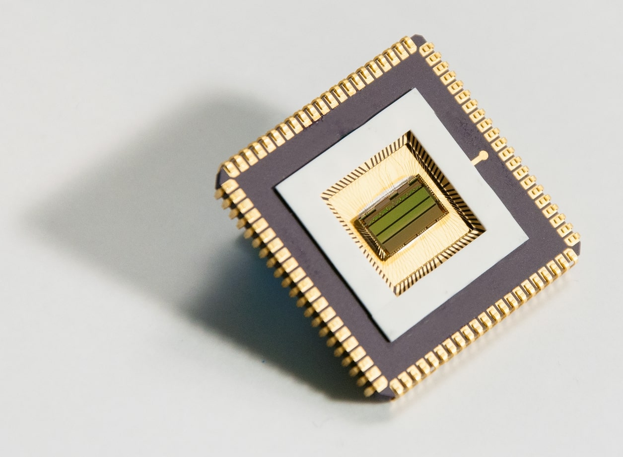
CSPAD sensor SPADEye2 in package
© Fraunhofer IMS
The SPADEye2 can detect and count single photons in two lines with high time resolution.

SPADEye2

The SPADEye2 line sensor offers extremely low-noise CMOS integrated SPADs in 2x192 pixels, which, combined with complex circuitry, allow time-resolved detection of photons. Each pixel contains an independent TDC (time-to-digital converter) for time detection and a circuit for counting incident photons. 4 SPADs in each pixel are connected by an adaptive photon coincidence circuitry for background light suppression. The SPADEye2 sensor can detect photons with a time resolution of 312.5 ps in a measurement window of 1.28 µs, theoretically covering a distance of 192 m at a resolution of about 5 cm.

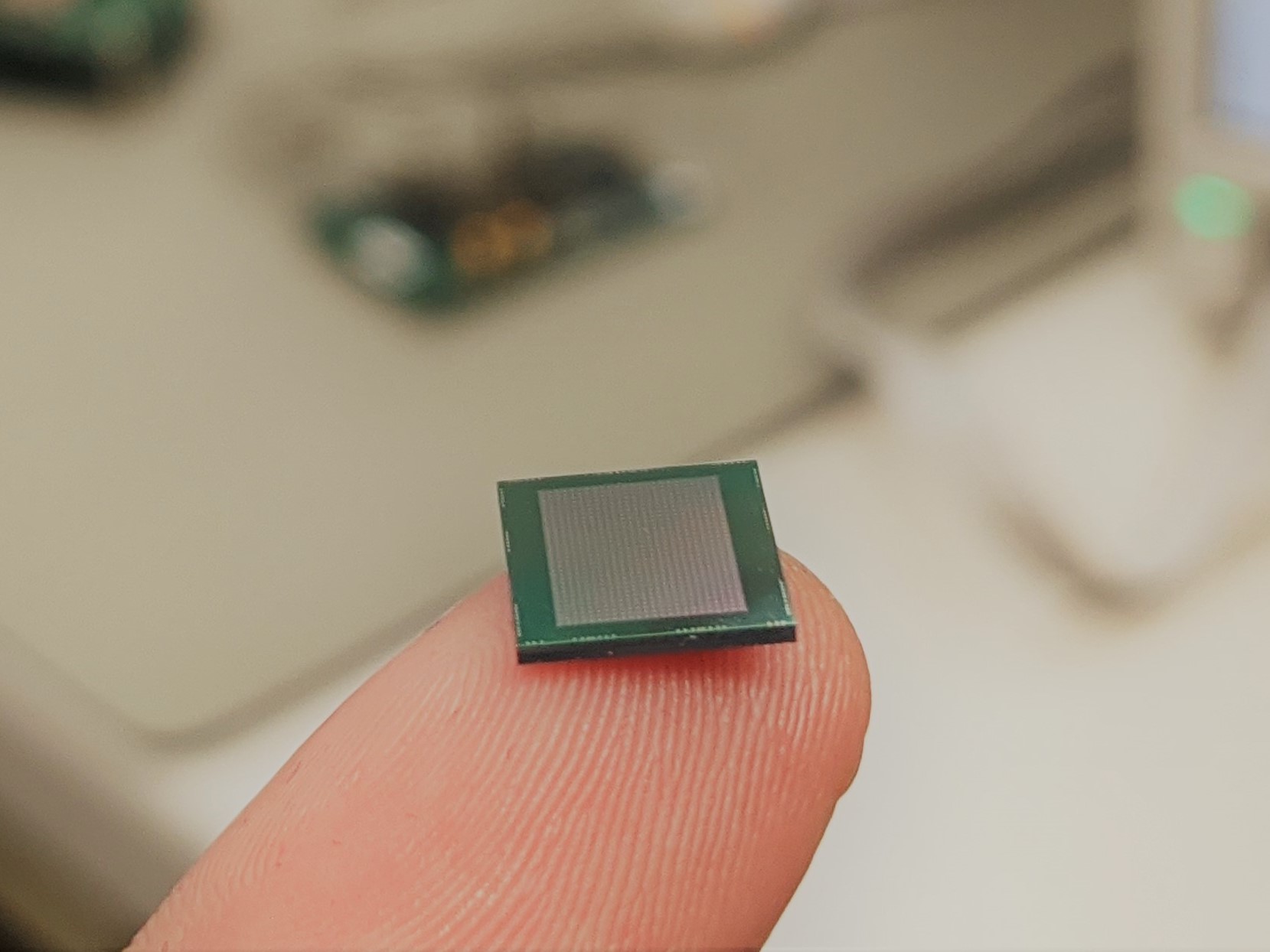
Sensor CSPAD αlpha on a finger
© Fraunhofer IMS
The CSPAD αlpha combines 3D integration and back-illuminated SPADs into a compact and high-performance image sensor.
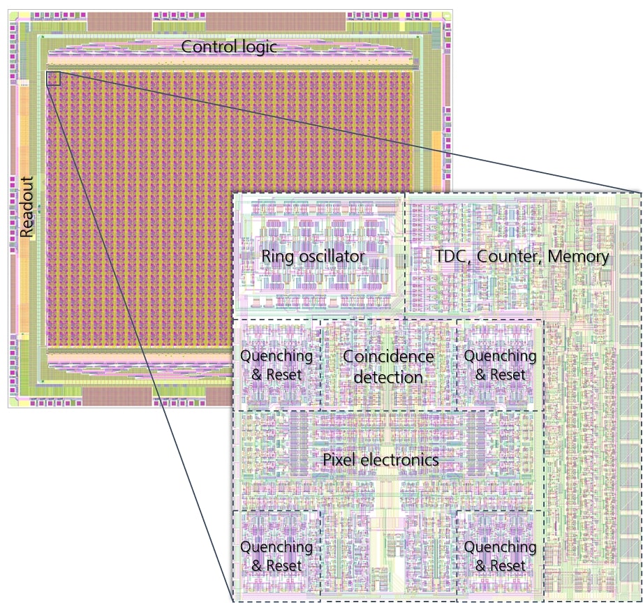
Layout of the CSPAD αlpha sensor with breakdown of circuit components.
© Fraunhofer IMS
The circuit components for the read-out electronics of the CSPAD αlpha are individually contained in every pixel.

CSPAD αlpha

The CSPAD αlpha marks an important milestone in the development of smart CMOS sensors and demonstrates a new form of integration of single-photon avalanche diodes (SPAD) into CMOS. The CSPAD αlpha combines for the first time the highly sensitive sensors with their electronics in the form of a three-dimensional chip stack. Using the 8" wafer-to-wafer bonding technology developed at IMS, high-resolution pixel matrices can be integrated with fast readout electronics in a very small space. CSPAD αlpha demonstrates the quality of this new 3D stacking method with its LiDAR capabilities and forms the basis for further chip designs.

With 32 x 24 pixels, distance measurements can be performed using only one illumination (flash LiDAR) and a 26 kHz readout rate. The TDCs (time-to-digital converter) are integrated for every pixel in the electronic part and enable a time resolution of less than 420 ps. By using microlens arrays, an additional 7-fold improvement in sensitivity can be achieved. In a further development, the area sensor CSPAD3k with an improved resolution of 64 x 48 pixels is currently being fabricated.

The Fraunhofer IMS is continuously working on the development and optimization of SPAD-based sensors and is looking for partners for applications of the CSPAD sensors. Our evaluation kits offer easy access to the sensors for any application with many possibilities for customization.

If you need more information or are thinking about a custom CSPAD sensor, please contact us.

ATLAS - Fraunhofer IMS LiDAR Target Emulator

ATLAS - Fraunhofer IMS LiDAR Target Emulator for object and environment detection revolutionizes driver assistance systems.

Next Level Photonics

Novel methods for generating and detecting light together with our partner Kyoto University

SPADEye2

2 x 192 pixel SPAD sensor with in-pixel TDC and adaptive coincidence 

Owl

LiDAR camera as platform for evaluation and demonstration of 3D sensors

CSPAD αlpha

Further information about the CSPAD αlpha is available on request!

UTOFIA

QVGA ToF sensor for a compact and cost-effective underwater camera

Our technologies - Innovations for your products

High-Speed Imaging

High-resolution and high-frequency optical sensor systems allow ultra-fast measurements of profiles and surfaces

Low Light Detection

Highly sensitive image sensors can detect single photons with spatial and temporal resolution without loss of information

Our technology areas - Our technologies for your development

Integrated Sensor Systems

Covers all electronic components for sensor signal conditioning and readout.

Optical Systems

Comprises 3D-Sensors, High-Speed-Imaging, detection of extreme low light as well as scientific imaging.

Wireless and Transponder Systems

Incorporates the wireless acquisition of sensor and ID-data even in passive systems.


Smart Sensor Systems

Here you can get back to the overview page of the core competence Smart Sensor Systems (SSS).