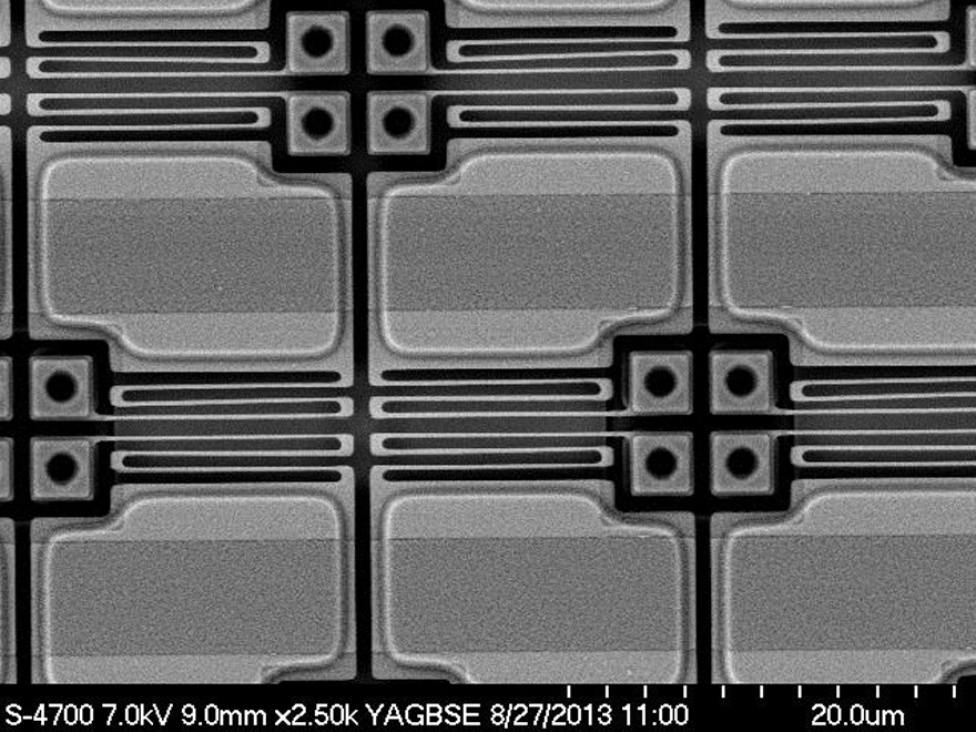


The development of customer-specific uncooled infrared sensors at Fraunhofer IMS in Duisburg is realized using several technologies. The developed uncooled infrared sensors (IR imagers) are based on microbolometer technology for applications in wavelength ranges of 3 µm to 5 µm or 8 µm to 14 µm. The microbolometer as a sensor element of an uncooled IR imager works according to the thermal principle. Here, the incident IR radiation is absorbed by a sensor membrane and due to a very good thermal insulation converts it according to the incident power into a temperature increase and the relating change in resistance.
Fraunhofer IMS has developed its own manufacture process for microbolometers as its core competency und is the only manufacturer of microbolometers in Germany. For the readout technology of these microbolometers Fraunhofer IMS has developed a CMOS readout circuit that converts the change in resistance due to temperature into digital values by using a large number of ΣΔ-ADC simultaneously. The digital and low-noise readout of microbolometers is produced in the in-house clean room using a 0.35 µm CMOS technology.
Microbolometers as sensor elements of uncooled infrared sensors work according to the thermal principle and therefore have to work in a vacuum housing for the reduction of thermal losses due to gas convection. Fraunhofer IMS has realized the smallest vaccuum housing possible for uncooled IR imagers with the development of the vacuum chip scale packages technology (CSP). The vacuum chip scale package contains an IR transparent window with anti-reflective layer and exhibits, apart from the size benefits, also cost benefits due to the integrated manufacturing process.
Based on these technologies: the microbolometer technology, the digital readout circuit and the vacuum chip, Fraunhofer IMS has developed a digital IRFPA (infrared focal plane array) with QVGA resolution and 17 µm pixel pitch. Thereby, the development of compact, efficient and easy to use IR imagers has been performed successfully.
On the basis of this digital IRFPA, Fraunhofer IMS has realized the world’s first infrared line sensor with 340 pixels. The number of lines is digitally customizable (2-256 lines).
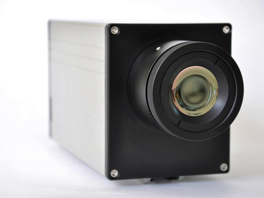
For testing of the IRFPA for customers Fraunhofer IMS has developed an IRFPA-Kit. This IRFPA Eval-Kit enables new users to put the IR imager into operation quickly and to evaluate. For this purpose is is constructed as an IR camera consisting of optics, recording of the IR imagers, interface electronics and operating software. The modular setup of the IRFPA allows for adaptions to different variants of the IR imagers produced at Fraunhofer IMS.