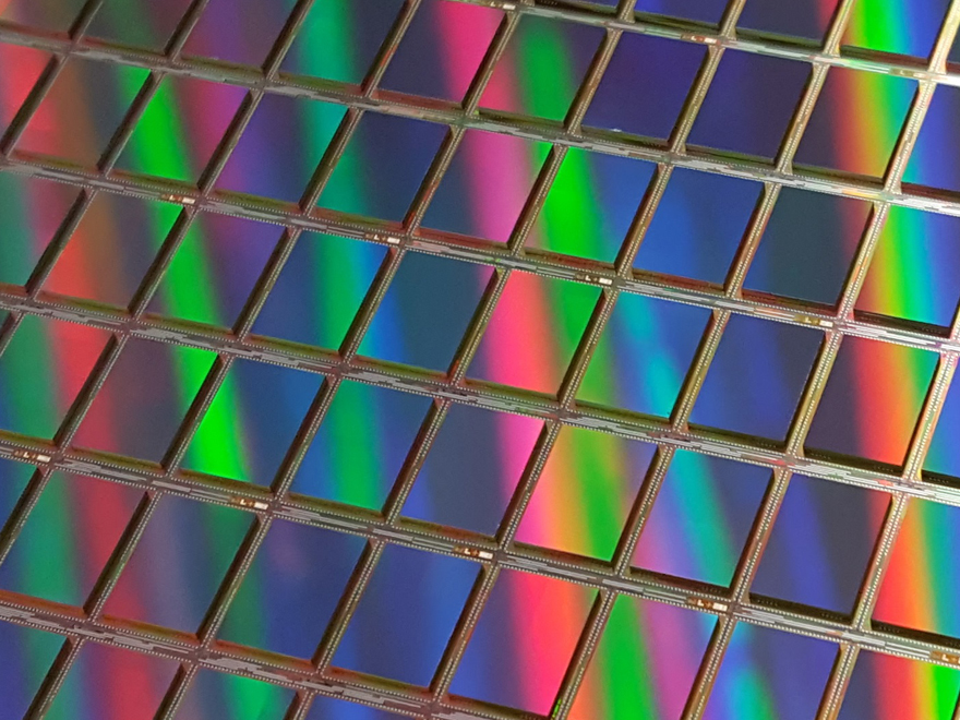
Fraunhofer IMS has realized the smallest vaccum housing possible for uncooled IR imagers with the development of a vacuum chip scale package (CSP) with an integrated infrared-transparent window. Microbolometers as sensor elements of an uncooled infrared sensor work according to the thermal principle and therefore have to work inside of a vacuum housing to reduce thermal losses caused by gas convection. This vacuum chip scale package includes an IR-transparent window with an anti-reflective coating and shows advantages not only in scale, but also in cost reduction through the integrated manufacturing process. The technology of the vacuum shcip scale packages can be used universally for vacuum and protective housing in applications other than uncooled infrared sensors.
The vacuum chip scale package consists of CMOS substrate in its lower part, which includes the readout circuit (ROIC) and the microbolometer array. The electrochemically separated solder frame is surrounding the microbolometer array. Using a flip-chip-process, an IR-transparent cover is placed onto the soldering frames with a broadband double-sided anti-reflective coating. On wafer scale, a vacuum soldering process takes place in which the soldering frames are sealed hermetically with the IR-transparent cover und therefore realizing a micro-cavity with a good vacuum level around the microbolometer array. To guarantee the vacuum level and the long-term stability, a getter on the insider of the cover is activated during the soldering process.
Through this form of the optimized wafer level process there are significant cost benefits to the realized vacuum hosuing in comparison to the classic wafer level package in which every substrate wafer needs its own cover wafer. In the Fraunhofer IMS developed vacuum chip scale package the IR-transparent covers are only placed on successfully tested readout circuits. Also, the size of the IR-transparent cover can be optimized independent from the size of the readout circuit resulting in more IR-transparent covers on a cover wafer than included by a substrate wafer readout circuit. Even the sawing process for separation of the readout circuits of the substrate wafer is simplified, because the wheel rim for the electrical connection of the readout circuit do not need to be elaborately exposed over sawing steps.
The whole manucturing process of the chip scale packages is done in the microsystem technology Lab&Fab of Fraunhofer IMS on 200 mm wafers. Both customer provided wafers of Fraunhofer IMS produced wafers can be used for this. The covers used for the encapsulation can also be manufactures and adapted to the target application by Fraunhofer IMS. Through the suitable choice of cover size the bondpads of the micro system chips can be readily accessible after the production of the chip scale package, making a functional test possible on wafer level and facilitating the choice of chips for further processing after separation.
