Uncooles infrared sensors use microbolometers as sensor elements for IR radiation. Fraunhofer IMS has developed its own manufacturing process for microbolometers as a core competency and is the only manufacturer of microbolometers in Germany. Microbolometers work according to the thermal principle in which the emitted infrared radiation from an object is absorbed via a thermally insulated membrane. This mebrane warms up due to the thermal insulation and the absorption. Because the membrane contains a temperature dependent resistance as a sensor layer, a change of the electrical resistance takes place, which is converted into a 16-bit signal of the readout circuit. The sensor materials used globally are vanadium oxide or amorphous silicon. The uncooled infrared sensors of Fraunhofer IMS are based on amorphous silicon.
An important parameter for microbolometers is their pixelpitch which is defined as the center to center distance of microbolometers. Uncooled infrared detectors mostly feature a pixelpitch of 25 μm, 17 μm, or 12 μm.
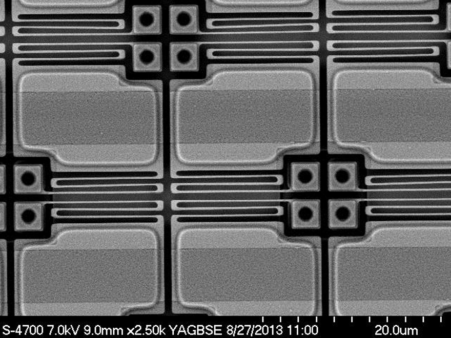
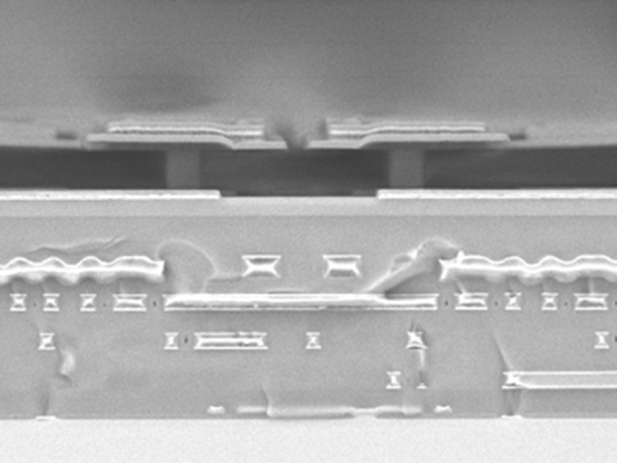
The microbolometers are produced using postprocessing steps on CMOS wafers in the MST Lab & Fab clean room of Fraunhofer IMS. The following images show the top view and the cross section of two scanning electron microscope images of a realized microbolometer.
The left SEM image shows the top view of a microbolometer structure with 17 μm pixelpitch. In the center the absorption membrane is visible. In the corner two metal contacts are placed for the connection of the readout circuit (ROIC). Two bridges for thermal insulation of the membrane are realized between the membrane and the contact.
In the right SEM image the cross section of a microbolometer und the underlying readout circuit are depicted. The membrane is fixated about 2 μm above the reflective layer using both bridges. It forms a λ/4 resonator which provides the maximum absorption of the incident IR radiation. The depicted microbolometer structure is a so-called “single level” microbolometer which can be manufactured using a single sacrificial layer process. The readout circuit is below the microbolometer and has clearly visible metal pairs.

