

Experience and offers in the field of CMOS technology development at the Fraunhofer IMS
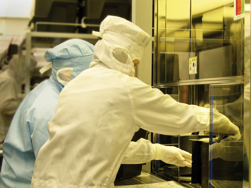
Fraunhofer IMS has more than 30 years of experience in CMOS technology development and a complete, professionally operated 200 mm CMOS line with various robust CMOS processes down to a development base with a structure size of 0,35 µm.
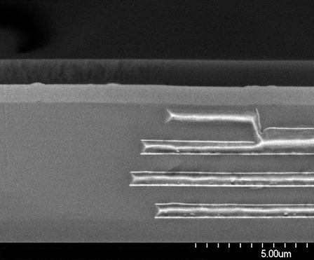
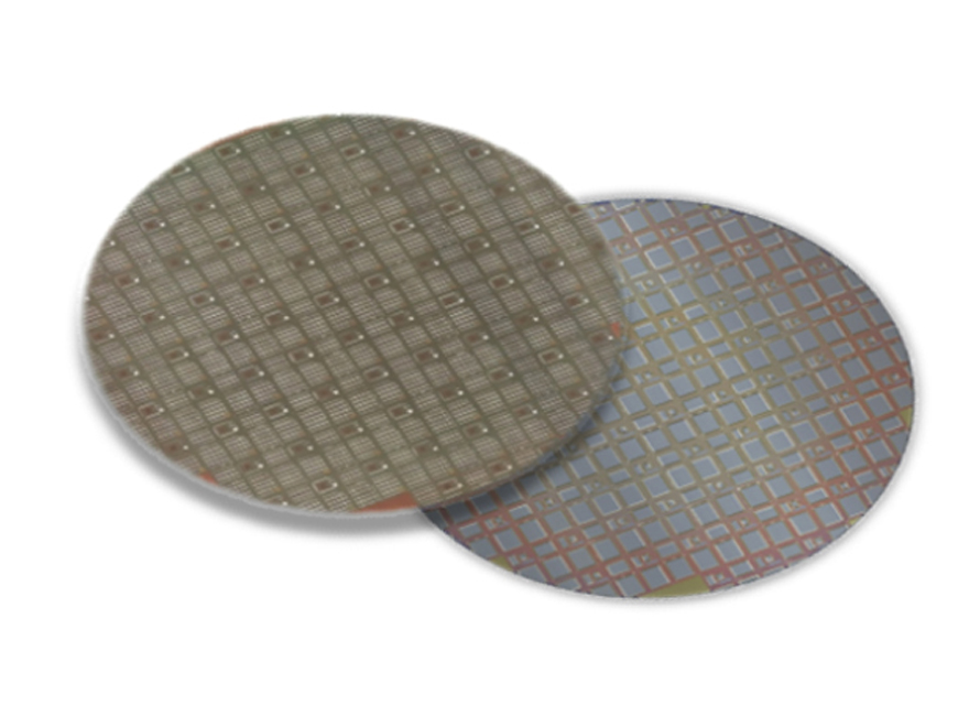
The IMS optimizes CMOS processes in the sense of the “More than Moore principle” by integrating additional functions such as high voltage resistant devices, high frequency circuits, sensors or by developing technologies that enable the use of the circuit under harsh conditions. The preparation of CMOS wafers as “intelligent” substrates by e. g. planarization is also an important development task. On these “intelligent substrates” layers are deposited and structured by post-CMOS processes to create new additional devices on the CMOS circuits.
Development of application- and customer-specific CMOS processes
Examples for the complete development of customer- and application-specific CMOS processes are the mixed signal 0.35 µm automotive CMOS process and high temperature (300°C) processes. Accompanying processes and component simulations (TCAD) as well as electrical characterization including parameter extraction and reliability investigations are part of the activities of Fraunhofer IMS.
Another important field of activity is the integration of special devices and process modules into our own or the customers CMOS processes. This also applies, for example, sensors in form of optically sensitive devices such as SPADs (Single-Photon Avalanche Diodes) or pressure sensors. Our further fields of activities are circuit devices like non-volatile memories (EEPROM or flash cells) including specific circuit development as well as high voltage devices. Special process modules for UV-transparent passivation and the removal of dielectric layers over a photodiode with subsequent deposition of an anti-reflective coating are also part of the Fraunhofer IMS repertoire.
Besides the integration into the CMOS, Fraunhofer IMS is also engaged in the development of CMOS compatible processes for discrete devices such as SiPM (silicon photomultiplier), DEPFET (depleted p-channel field-effect transistor) or DOEs (diffractive optical elements), which also includes the development of corresponding interconnection technologies such as double-sided wafer processing.
Post CMOS process for sensor integration
Planarized CMOS surfaces serve as the basis for post-CMOS sensor integration. In combination with "Micro-Electro-Mechanical Systems" MEMS or "Nano-Electro-Mechanical Systems" NEMS, sensor elements such as optical, mechanical, physical, chemical and bio-sensors can also be realized. Examples are uncooled bolometer arrays and nanowire gas sensors. The combination of CMOS and MEMS (or NEMS) results in innovative and extremely compact microsystems for use in medicine, industry, automotive, aerospace and consumer applications.
