 Fraunhofer Institute for Microelectronic Circuits and Systems
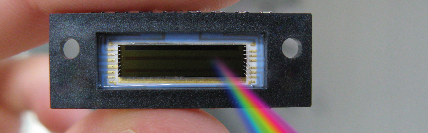
CMOS and MST manufacturing with highest quality


Fraunhofer IMS offers an extensive infrastructure and numerous options for the development, manufacture and characterization of sensors.
The 0.35 µm CMOS technology installed in the Fraunhofer IMS is qualified according to the automotive standard ISO TS16949 and therefore extremely stable and reliable. Special CMOS "Opto" options enable the realization of special process steps and components such as CCDs or SPADs.
After CMOS processing, the 200 mm wafers can be further "refined" in the MST Lab&Fab. Further process steps such as wafer bonding, planarization, thinning, deposition of various materials and photo technology are possible as well. This enables, for example, the implementation of color sensors, backside illumination (BSI) anti-reflection coating or chip-scale packaging.
Further clean rooms are available for testing prototypes and products as well as for assembly and connection technology.
In our measuring laboratory we characterize and test the prototypes of the newly developed optical sensors with our professional measuring stations both in the wafer compound and in the packaged state.