This leads to a significant acceleration of charge collection compared to conventional diffusion-based detectors and makes this device an ideal candidate for high-speed applications such as 3D time-of-flight imaging. Here, the reflected light can be measured via two individually adjustable integration windows and the distance to the object can be calculated via the integrated signal. The accumulation of the charge carriers in the pixel reduces noise influences and allows multiple light pulses to be detected in one image. Both the integration times and the accumulation number are adjustable, so that an optimal adaptation to the necessary measuring distance and the light source used can take place. In addition, the background signal can be suppressed, either by an additional measurement or an additional integration window. Of particular advantage with this ToF sensor is the possibility to develop laterally high-resolution detectors.
The silicon-based photosensitive pinned photodiode (PPD), which enables the detection of visible and near-infrared light radiation and can convert it into an electric current, is one example. It is a photodetector structure used in almost all CCD and CMOS image sensors (CIS) due to its low noise, high quantum efficiency and low dark current.
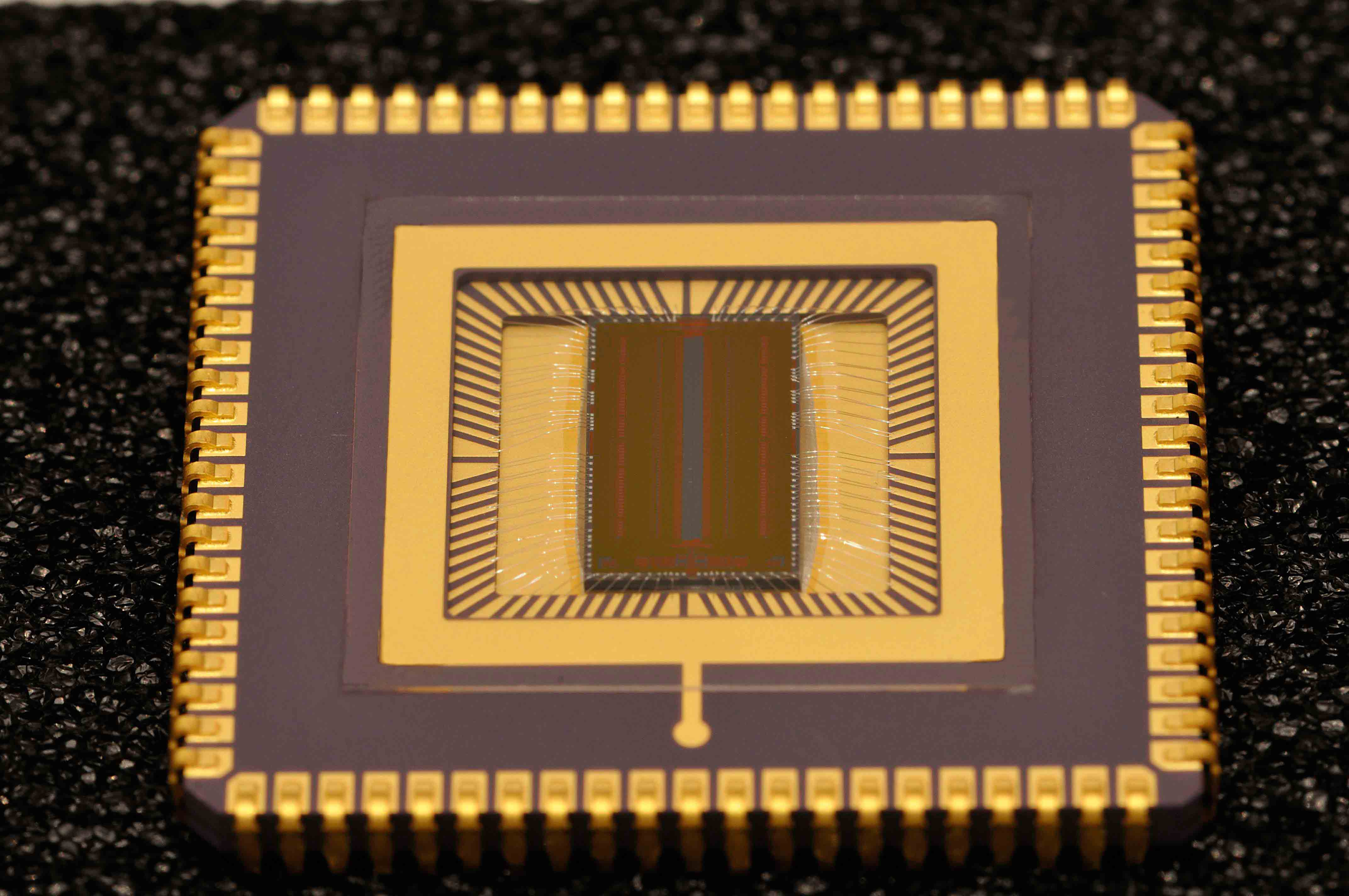
Another specialty of the Fraunhofer IMS are ultrafast line sensors. These enable the rapid optical inspection of surfaces and they are therefore ideally suited for quality inspection in industrial manufacturing and for determining the condition of objects such as railroad tracks. The 60-line high-speed sensor is twice as fast as currently available solutions and at the same time delivers high-quality images in very high resolution. Each line of the sensor consists of 2016 pixels with a pixel pitch of 9µm. The horizontal fill factor is close to 100%. Per second, the high-speed sensor captures up to 200,000 color images and up to 600000 black/white images at exposure times of a few millionths of a second.
In addition to design, we offer our customers special services in wafer post-processing, process optimization and electro-optical characterization. Furthermore, special process options such as
- stitching
- UV-transparent passivation
- planarization
- color filters
- microlenses
are available for product development.

