 Fraunhofer Institute for Microelectronic Circuits and Systems
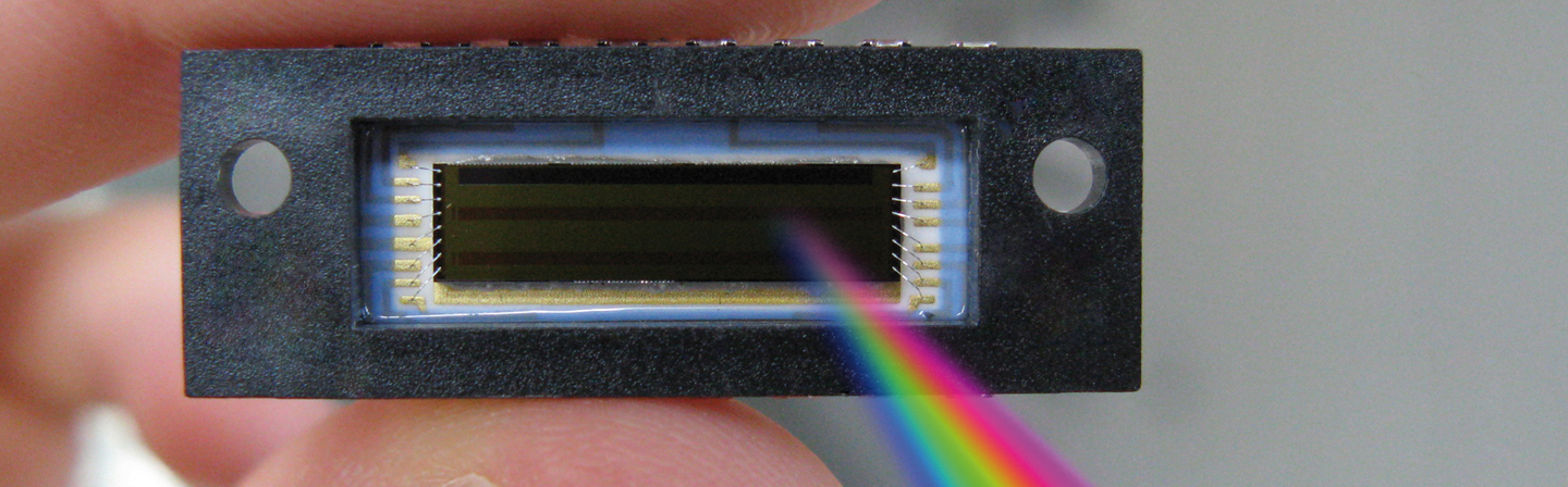
Highly dynamic CMOS-CCDs in Fraunhofer IMS in-house process

Conventional CCD technologies for optical sensors are mainly used where high demands have to be met by the sensor:
- Applications that require an extremely low dark signal
- Applications with Time Delay Integration (TDI) (e.g. space detectors)
Usually, for this kind of sensors a highly pure, low-defect silicon material is used as a basis to minimize crystalline as a cause for parasitic dark signals. The dynamic range in the upper part is achieved by operating voltages that allow more than 10 V differences in potential and therefore enable the transport of large load units.
One of the significant disadvantages of a CCD not integrated into a CMOS is that the complete signal processing as well as the sensor control has to be carried out externally. This leads to considerable parasitic effects, for example high line resistance or bond wire inductivities. Another disadvantage is that the pixel values need to be transferred over a very fast analog CCD shift register to the exit. Through these high losses the power consumption for a conventional CCD are much higher than for the CMOS-CCD.
Fraunhofer IMS has developed a process in which CCDs are integrated into the CMOs process in a way that allows the CMOS-CCDs to use the advantages of both technologies:
The integration of the CCD into the CMOS process enables the direct parallel signal processing and AD conversion on the chip and therefore minimizes the parasitic disruptive effects. The output of the digital data over several channels removes the bottleneck in data transfer.
The adaption of the process to the voltages typically used in CCDs allows for the processing of big load units.
A specially tailored gate structure from the two overlapping polysilicon gates guarantees a continuous potential curve inside of the CMOS-CCD and enables a low-loss charge transport, especially for small signals.
Through a deep channel implantation in the CMOS-CCD the charge transport is kept from the interface and therefore ensures a high transfer efficiency.
The main application area for CMOS-CCDs is the area of TDI space detectors. For this application sensors with very high optical requirements are needed that exhibit a low power input at the same time to keep weight and costs for sensor climate control low.