 Fraunhofer Institute for Microelectronic Circuits and Systems
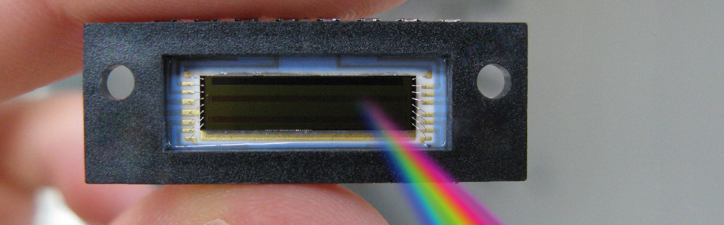
Highly sensitive line sensors in Fraunhofer IMS in-house process

The optical spectroscopy is a basis technology with great leverage in the industrial and scientific sector, where it helps with increasingly accurate analyses of materials, with developing new processes, optimizing and controlling manufacture processes or detecting contamination in the environment or food. The characteristic wavelengths of many elements are in a short wavelength range of the spectrum, which means that the corresponding photo sensors in this range need to be highly sensitive. Today photo sensors that are based on the CCD technology (Charge Coupled Device) are used. CCDs are due to their principle not able to suppress the excitation pulse in one of the most important spectroscopic techniques (emission spectroscopy in which the excitation occurs by laser or electric sparks). This leads to the measurement signal being dominated by the excitation pulse in a high degree und therefore highly restricting the dynamics of the usable signal. Thus, the detection threshold for elements with a low concentration is decreased significantly.
Fraunhofer IMS offers an alternative with its CMOS technology that is able to solve these problems. The benefits contain the possibility to realize very fast sensors and a large variety of detectors with different properties (high sensitivity, low noise, high dynamics, to name a few), to carry out complex signal processing directly on the chip and also in the cost-effective production. The short wave spectral range of UV (380-200 nm) and vacuum UC (200-100 nm) is of primary importance in the spectroscopic analysis. This way, in this wavelength range the characteristic lines of selenium (193 nm) and arsenic (around 197 nm), phosphorus, Sulphur, carbon in the range of 165 nm and the halogens (Cl, Br, iodine, up to 120 nm) can be found. These spectral ranges are detected by Fraunhofer IMS special process steps by thinning and anti-reflective coating.