 Fraunhofer Institute for Microelectronic Circuits and Systems
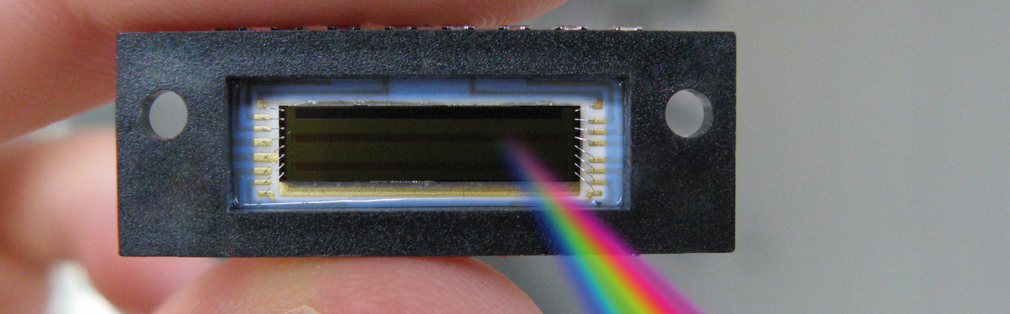
")
Backside illumination sensors (short: BSI sensors) are characterized by their increased image quality and therefore essential in entertainment electronics and in smartphones. With the introduction of the wafer-to-wafer (W2W) process Fraunhofer IMS reaches a new technology level that enables the production of high-quality BSI sensors. First photodetectors and the corresponding read out circuits are separately manufactured on 8’’ wafers. Next, both wafers are connected in a permanent way. This creates especially compact setups with the shortest electrical connections.
This heterointegration is applied in particular in the production of high-quality 3D environmental sensors with SPADs (Single Photon Avalanche Diodes). The highly sensitive photodiodes allow for high temporal resolution for the detection of object distances and are therefore in use in LiDAR sensor systems for autonomous driving. With BSI technology 2D SPAD matrices can be generates that exhibit very high fill factors of up to 70%. This creates enormous advantages in the use of the detectors as LiDAR sensors in traffic.
At Fraunhofer IMS the complete process chain for the manufacture of the sensors is available. Engineers with long process experience in CMOS and/or MEMS process are complemented by their colleagues from integrated circuit packaging, circuit design and test. The cooperation of all areas in one location is a unique selling point of Fraunhofer IMS.
The independent production of read out circuits and photodetectors allows for an optimal selection of wafer materials with regard to sensor requirements. 8’’ wafers from the in-house CMOS line or from external semiconductor manufacturers can be integrated with the photodetectors. Fraunhofer IMS uses their in-house 0.35 µm OPTO process and can rely on 30 years of CMOS experience.
Contact us and look into the world of BSI sensors from Fraunhofer IMS!