Due to the continuous progress of miniaturization, reliability is becoming an ever greater challenge. Both at device and system level, this results in extreme requirements for future complex applications. Above all, reliability must be guaranteed in new and critical environments, where electronics are being used more and more frequently. This applies in particular to the forward-looking areas of transportation, mobility, energy and digital industry in Germany.
One forward-looking application in the field of mobility is autonomous driving, where the use of high-resolution LiDAR systems is essential. With the sub-project "Reliability of optical sensors using the example of a LiDAR detector", the Fraunhofer IMS is making an important contribution to the joint project "Intelligent Reliability 4.0" - iRel 4.0 for short - and is thus also strengthening the strategic further development of LiDAR technology at the institute.
In iRel 4.0 - a project funded by the European Industry Partnership ECSEL-JU and the BMBF - the improvement of the reliability of components and systems along the value chain chip-package-board/system over the entire life cycle is to be addressed as a central topic.
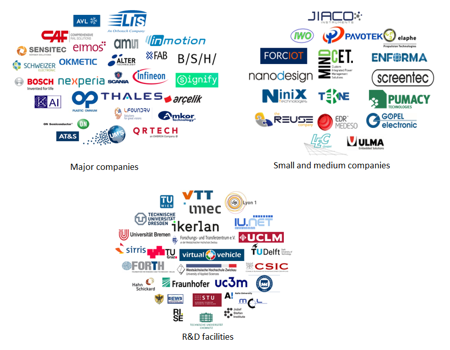
To achieve the strategic goals of the joint project, 75 cooperation partners from 14 European countries are working together. Among them are well-known large semiconductor manufacturers, end users, as well as research institutes and universities (for an overview of the cooperation partners see chart below). The Fraunhofer Gesellschaft is represented in the consortium by 7 institutes (IIS/EAS, ENAS, IFAM, IISB, IMS, IMWS, IWS/AZOM). The project duration is 3 years, the total budget is about 103 million euros.
Fraunhofer IMS is a very experienced cooperation partner for the consortium due to more than 35 years of experience in the field of microelectronic circuits and systems.
Within the joint project, the contribution of the Fraunhofer IMS is generally focused on the development and expansion of scientific expertise in the field of electronic reliability. Thus, the Fraunhofer IMS will address aspects of the reliability of optical sensors within the subproject. The work is partially embedded in the Use Case T-4 "Backside Illuminated Optical Sensor", which is led by Elmos Semiconductor SE and deals with the reliability of LiDAR detectors.
Use Case T-4 focuses on the manufacturing process and reliability prediction of backside illuminated optical sensor systems. The entire manufacturing chain is considered. This starts with the design of the sensor and the associated readout circuitry and continues with fabrication, wafer bonding, packaging and electro-optical testing.
Contribution of the Fraunhofer IMS to increasing reliability
The core task is to improve the reliability of BSI sensors (BSI - Backside Illumination). This includes on the one hand the optimization of the manufacturing process to reduce technical failures over the product lifetime (contribution to work package 3), and on the other hand the realization of an automatic wafer level test to be able to check electro-optically relevant parameters on production level and to enable an even more accurate chip characterization (contribution to work package 5).
Optimization of the BSI manufacturing process
The manufacturing process provides for 3D integration to connect optical sensors and CMOS circuits. Only in this way is a highly symmetrical connection of the runtime-critical signals for evaluation possible. For this purpose, Fraunhofer IMS is developing a wafer-to-wafer (W2W) approach, whereby sensor and circuit wafers are planarized after respective CMOS fabrication and are connected over the entire surface via "direct oxide bonding". To increase the reliability of W2W fabricated BSI sensors, a detection of voids for wafer bonding with a surface acoustic microscope (SAM) will be optimized and introduced into the fabrication process to obtain a quality parameter for the wafer bonding process that can be used for further optimization. For example, one aspect of reliability that is being investigated in this project is ensuring that sensor and circuit wafers are testable prior to planarization and bonding process.
To establish contact between the individual wafers, "micro-vias" are implemented. This is a process module that combines classic silicon deep etching (DRIE - Deep Reactive Ion Etching), isolation and metallization.
The realization of backside illumination of sensors requires precise thinning of the sensor wafer. Even after further processing of the sensor wafer (lithography, production of the through-hole plating between sensor and readout wafer), an optically smooth and clean surface is essential for functionality. Both aspects are difficult to achieve with conventional grinding and etching processes of silicon wafers. Precise stopping on the low-doped device film silicon surface with a reproducible residual thickness is addressed by developing a wet etch process suitable for high-quality epitaxial substrates.
The optimized manufacturing process will be offered to potential project partners as a service through licensing.
Optimizing reliability by introducing automatic wafer-level testing for LiDAR sensors
Currently, no standard wafer level test for different electro-optical parameters is available. As a further core task, the Fraunhofer IMS will develop an innovative fully automated wafer level test for a LiDAR detector as an example of an integrated optical sensor, which includes dedicated test hardware and simulates optical environmental conditions. A central component is the illuminator, which illuminates the optical sensor with homogeneous irradiation according to EMVA standard 1288. The illumination can be used to determine the photon detection probability (PDP) as a measure of the sensitivity of the individual pixels. Other important parameters for LiDAR detectors include the dark count rate (DCR), which represents the background noise, and the temporal precision of the photon detections, which is based on the quality of the time-to-digital converter (TDC). With knowledge of these important specifications, early decisions can be made as to which chips are particularly suitable for further use, e.g., as part of a LiDAR system for autonomous driving. High-speed testing Full automation is one of the main focuses of the development of the test procedure. The test procedure to be developed will be able to be used as a platform for electro-optical characterization of different LiDAR detectors for German and European project partners.
The following overview shows the project partners from the "iRel 4.0" consortium:


