High Temperature SOI CMOS Technology (H035)

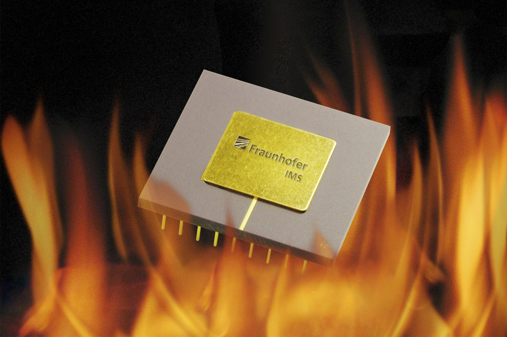
Fraunhofer IMS provides a high temperature resistant Silicon-on-Insulator (SOI) CMOS technology.

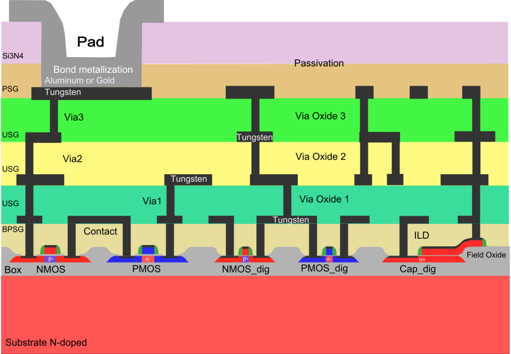
The picture shows a cross section through the H035 technology of Fraunhofer IMS
© Fraunhofer IMS
Depiction technology cross section H035

Fraunhofer IMS has more than 30 years of experience in CMOS technology development and operated as development and production basis a complete 200 mm CMOS line with different robust CMOS processes up to a minimal structure of 0.35 µm.

In this line there is a specific high temperature resistant Silicon-On-Insulator (SOI) CMOS technology available. Individual transistors are not isolated via diodes (pn junctions), but dielectrically by a buried oxide, reducing leakage currents by up to three magnitudes. An additional optimization of the devices enables a performant operation of integrated circuits in up to 300 °C. To increase the reliability even further and to reduce the degradation of electromigration the technology is also equipped with tungsten instead of the commonly used aluminum metallization. The minimal structure size of 0.35 µm and up to four metal layers allow for the realization of compact integrated systems including small embedded microcontrollers.
Technology overview of the high temperature SOI CMOS processH035

Parameters

Typical Values

Gate oxide (Thickness)
Analog
Digital

40 nm
9.4 mm
Minimal gate length
Analog
Digital

1.00 µm
0.36 µm
Maximal gate voltage
Analog
Digital

12 V (briefly 16 V)
3.6 V
Threshold voltage Vtn/Vtp  
Analog 25 °C 1.0 V/-1.6 V (@VBG=-5 V)
          250 °C 0.8 V/-1.3 V (@VBG=-5 V) 
Digital 25 °C 0.85 V/-0.85 V
          250 °C 0.6 V/-0.6 V


Subthreshold slope

(mV/Decade)

NMOS/PMOS
Analog 25 °C 100/160
          250 °C 340/440
Digital 25 °C 90/100
          250 °C 200/220
MOS reverse current @250 °C
NMOS analog
NMOS digital
PMOS analog
PMOS digital

1.0 nA/µm width
5.0 nA/µm width
0.15 nA/µm width
0.5 nA/µm width
Amount of metallization layer 4
Silicon film thickness 200 nm
Buried oxide (thickness) 400 nm
SOI MOS characteristics partly depleted
Resistance (Polysilicon)

(HighRes)
260 Ohm/□
100 ppm/°C
3.7 kOhm/□
Linear Capacity
Oxide thickness
Voltage dependency

45 nm
<100 ppm/Volt
EEPROM
Cell area/Bit
Data retention


Endurance

145 µm²
1000 h @ 250 °C
10 a @ 85 °C
1000 Cycles @ 250 °C
100,000 Cycles @ 25 °C

This may interest you

Integrated Circuits for Environmental Temperatures of up to 300 °C

Integrated circuits of high complexity for environmental temperatures of up to 300 °C in SOI CMOS

Overview Pages

High Temperature Electronics (Home)

At Fraunhofer IMS we develop integrated circuits, sensors and actuators in a 0.35 µm SOI-CMOS high temperature technology and manufacture them in our in-house clean room.

Applications

Conducted projects in the area of analog and digital circuit development for high temperature applications

Technologies

We develop integrated circuits and sensors of high complexity for environmental temperatures up to 300 °C in SOI CMOS.

Customer Benefits

In the business unit High Temperature Electronics Fraunhofer IMS offers an extensive catalogue of customer benefits from the concept study up to the production.

Download