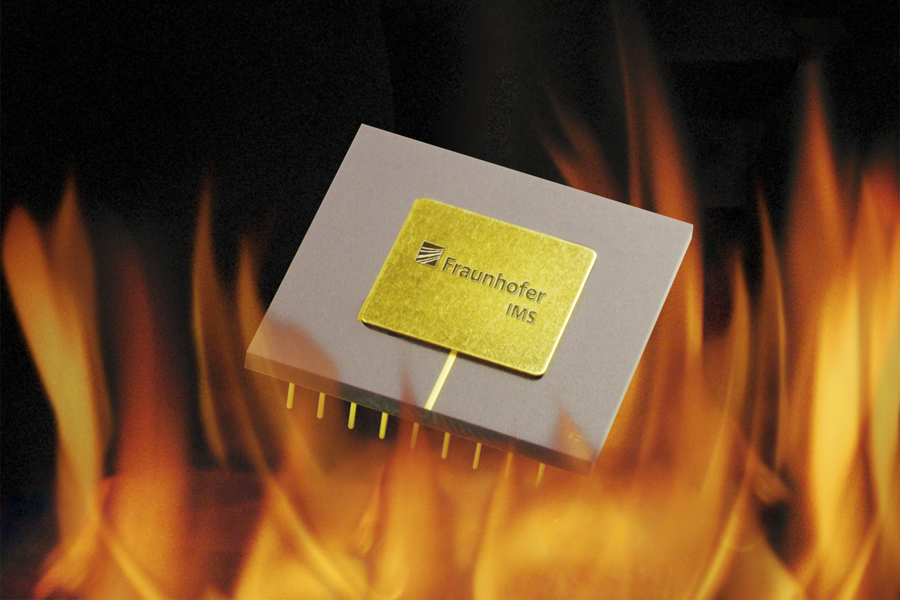
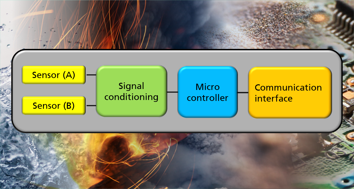
Within the framework of industry 4.0 there is an increase in monitoring of industrial processes with intelligent sensor systems. For this miniaturized, intelligent sensors for various physical quantities like pressure, vibration, acceleration or temperature are needed that can be embedded in a reliable and low-maintenance way in extremely harsh environmental conditions. In addition to the mechanical and chemical load there are other challenges, especially the application of such systems in an extremely large temperature range of -50 °C up to 300 °C and more. Examples for these applications are jet engines in aerospace or deep drilling for the geothermal sector as well as the development of fossil energy sources.
The 0.35 µm SOI CMOS high temperature technology provides the technological foundation for the production of complex integrated circuits for the mentioned temperature range.
Moreover Fraunhofer IMS offers an extensive range of know-how and services in the field of development of application-specific integrated high temperature circuits (high temperature ICs). A large team of experts with long years of experience in the area of circuitry and especially the very special requirements which comes with the operation in a large temperature range researches and develops high temperature ICs for various applications. Our expertise is both in the area of high-precision analog circuitry, for example for the extremely accurate evaluation of sensor signals and their signal processing, and the development of complex digital parts and memory modules.
We undertake the complete development projects or support you in the development of high temperature ICs, which are tailor-made for your application, over the chip design up to the production of pilot and small series. For this, there is an extensive PDK for the H035 process available including a digital standard cell library for the synthesis of HDL description (VHDL, Verilog). Existing analog circuit blocks like controllers, bandgap references, oscillators or ADCs can be integrated in your high temperature IC design as required and therefore decrease the design risk and the development time.
The in-house backend area allows for the fully automated test of your high temperature ICs both on wafer and component level.

