 Fraunhofer Institute for Microelectronic Circuits and Systems
Chip scale packages: The small packaging expert of Fraunhofer IMS
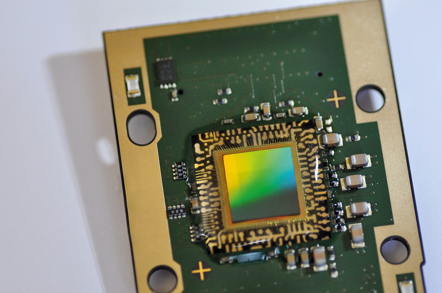
A strong case surrounds the fragile core: The new chip scale package (CPS) of Fraunhofer Institute for microelectronic circuits and systems IMS in Duisburg protects the sensitive sensors. The midget out of silicon has many talents: he is barely bigger than the chip itself, cost-effective and is producible in large quantities.
The chip scale package of Fraunhofer IMS is used where a vacuum or hermetically package as protection for dust and moisture is necessary. The small packaging expert is constructed for the house-made far infrared sensor. This sensor consists of fragile structures and does only work in vacuum. Therefore a package that causes as little as possible heat loss is necessary. Far infrared sensors are used for example in visualization of heat loss in buildings. They are used from the fire department in order to track sources of fire and from the automotive industry for night view assist. Chip scale sensors are able to package other sensors too, for example optical sensors as well as acceleration and rate sensors that are used in smartphones and consumer electronics.
How is a chip scale package constructed? Around the sensor that is going to be packaged is applied a flux-free solder frame made from metal. The solder frame is higher than the sensor and is locked with a cover. If for example a far infrared sensor needs to be packaged, the silicon cover is constructed especially permeable for the far infrared radiation. Beyond that the Fraunhofer IMS offers transparent glass covers for visual sensors or opaque covers for sensors that need to be protected from the light.
If there is need for a vacuum like with the far infrared sensors a getter enables and ensures this vacuum: the getter absorbs the gases that occur initially in the soldering process and later in the use of the sensor. Because of that the sensor can optimally function and even shows small temperature differences.
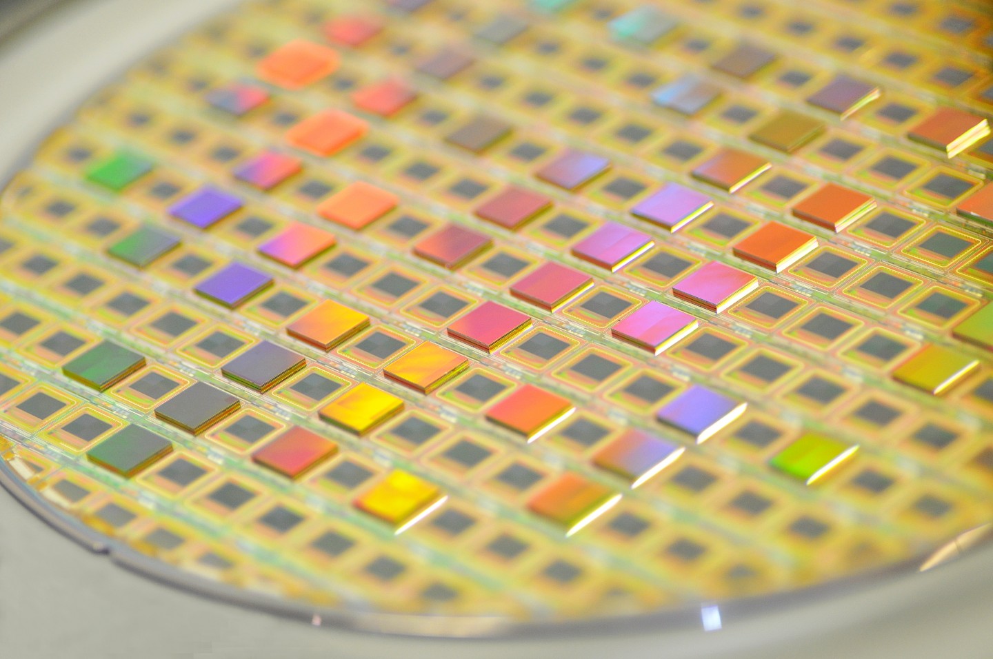
The various strengths of the chip scale packages are in the manner of manufacturing. The Fraunhofer IMS applies the cover with a chip-to-wafer-process (C2W) onto the sensors: The sensors are on a 200 mm wafer. The covers are built on a second 200 mm wafer, they are already sawed up there and then separately applied onto the sensors. In contrast to the wafer-to-wafer-procedure where first of all the sensor-wafers are connected with the cover-wafers and after that they are sawed up. “The C2W-procedure saves 30 to 50 percent material and therefore costs” explains Dr. Thomas Geruschke, module leader chip scale package at Fraunhofer IMS. It is especially noticeable in the procedure of large sensors.
Various factors lead to this large saving. Firstly on a wafer fit more covers then sensors – that saves material. Secondly only the sensors that passed the test of readout circuits are provided with a cover. And thirdly: At Fraunhofer IMS the sensors are tested again, already after they are provided with covers but before the wafers are sewed up. If the sensor does not pass the test he is not going to be built up any further (for example on a further plate). Even that saves material, time and money.
Another advantage of the procedure: the sensors are only isolated through the saw up of the wafer at the end of the process. “Impurities because of the sawing process play no longer a role because the sensor is already protected”, says Dr. Thomas Geruschke.
At the end of 2016 the procedure should be ready for series production of far infrared sensors. On request, the Fraunhofer IMS carries out adjustments of chip scale packages to other sensors.
The Fraunhofer Institute of Microelectronic Circuits and Systems IMS
Since 30 years scientists at Fraunhofer IMS in Duisburg deal with the development of microelectronic circuits, electronic systems, microsystems and sensors. Because of its comprehensive know-how, the access to technology and the high-quality development work the Institute is a worldwide recognized partner for the industry. In eight business units Fraunhofer IMS is dedicated to applied research, advance development for products and their applications. Stable, efficient and marketable technologies and procedures that are used in extremely many branches take center stage in contract work.
![Picture 2 [ JPG 10.72 MB ]](/content/dam/ims/en/images/Press/Press_Releases/2016/Chip%20Scale%20Package_Picture%202.jpg)